David Muller, the Samuel B. Eckert Professor of Engineering at the Cornell Duffield College of Engineering, who masterminded this ambitious project, emphasized the profound impact of this discovery. "Since there’s really no other way you can see the atomic structure of these defects, this is going to be a really important characterization tool for debugging and fault-finding in computer chips, especially at the development stage," Muller stated. This sentiment underscores the critical need for such a precise diagnostic capability in an era where electronic components are shrinking to atomic dimensions.
The semiconductor industry has long grappled with the challenge posed by exceedingly small structural flaws. As the complexity of computer chips has escalated and their constituent components have been miniaturized to the scale of individual atoms, even the slightest irregularities have the potential to disrupt the intricate dance of electrons that governs device operation. At the heart of every computer chip lies the transistor, a microscopic component that functions as an electronic switch, meticulously controlling the flow of electrical current. Each transistor features a channel, a pathway that opens and closes to regulate the passage of electrons. Muller eloquently likened this process to a fluid dynamic system: "The transistor is like a little pipe for electrons instead of water. You can imagine, if the walls of the pipe are very rough, it’s going to slow things down. And so measuring how rough the walls are and which walls are good and which walls are bad is now even more important." This analogy vividly illustrates how surface imperfections at the atomic level can directly translate to performance degradation.
Muller’s illustrious career has been dedicated to exploring the physical boundaries of semiconductor technology. His tenure at Bell Labs from 1997 to 2003, the very institution where the transistor was invented, was instrumental in his investigations into the ultimate limits of device miniaturization. In the early days of transistors, their arrangement on chips was primarily planar, spreading outwards in a fashion reminiscent of suburban development. However, as engineers encountered the limitations of available surface area, a paradigm shift occurred, leading to the vertical stacking of transistors. This innovative approach gave rise to complex three-dimensional architectures, analogous to the towering structures of modern apartment buildings.
"The problem is these 3D structures are smaller than the size of a virus. And these days, it’s a lot smaller. It’s more like a molecule-in-the-cell kind of scale," Muller explained, highlighting the astonishingly diminutive dimensions involved in contemporary chip design. Today’s advanced chips can house billions of transistors, and as their size continues its relentless descent, the task of diagnosing performance issues has become exponentially more arduous. Karapetyan further elaborated on this challenge: "These days, a transistor channel can be only about 15 to 18 atoms wide, which is super, super tiny, and they’re extremely intricate. At this point, it matters where every atom is, and it’s really hard to characterize." This statement underscores the critical need for tools that can resolve structures at this unprecedented level of detail.
The breakthrough in imaging capabilities is deeply rooted in advancements in electron microscopy. Earlier in his career at Bell Labs, Muller collaborated with fellow scientist Glen Wilk, now vice president of technology at ASM. Their joint research focused on finding alternatives to silicon dioxide, the prevailing gate material at the time, which suffered from excessive current leakage as devices shrank. Their work contributed significantly to the adoption of hafnium oxide, a material that subsequently became the industry standard for computer processors and mobile devices starting in the mid-2000s. Muller reflected on the impact of their earlier work: "The papers we published on how to use electron microscopes to characterize these materials, I can tell you, a lot of the semiconductor folks had read those very, very carefully." He added, drawing a stark comparison between past and present capabilities, "When we got back into this project, that was very clear. And the microscopy has gone a very long way. Back then, it was like flying biplanes. And now you’ve got jets."
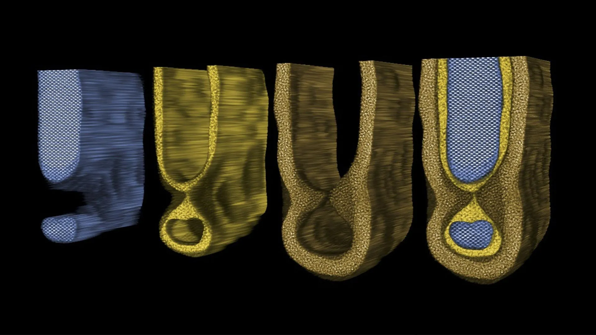
This metaphorical "jet" represents electron ptychography, a sophisticated computational imaging technique powered by the electron microscope pixel array detector (EMPAD). The EMPAD, a technology co-developed by Muller’s research group, meticulously records intricate patterns generated as electrons traverse the transistor structures. By analyzing the subtle shifts in these scattering patterns between different scan points, researchers can reconstruct remarkably detailed three-dimensional images. The precision of this system is so profound that it has yielded the highest resolution images ever captured, enabling scientists to visualize individual atoms with extraordinary clarity – a feat recognized by Guinness World Records.
The collaboration between Muller and Wilk was rekindled over 25 years later, this time with vital support from TSMC and its Corporate Analytical Laboratories group. Their collective objective was to apply the cutting-edge EMPAD technology to the rigorous demands of modern semiconductor devices. "You can think of this imaging technique like solving a massive puzzle, both in terms of taking the experimental data and doing the computational reconstruction," Karapetyan explained, likening the complex process to assembling an intricate jigsaw puzzle.
Following the meticulous collection and reconstruction of imaging data, the research team proceeded to precisely map the positions of atoms within the transistor channels. This detailed analysis unveiled subtle roughness at the interfaces of these channels, which Karapetyan vividly described as "mouse bites." These defects were found to form during the highly optimized growth processes employed in the manufacturing of these advanced structures. The research team utilized sample devices fabricated at the nanoelectronics research center Imec, which provided an ideal platform for rigorously testing and validating the imaging technique. "Fabrication of modern devices takes hundreds, if not thousands, of steps of chemical etching and deposition and heating, and then every single step does something to your structure," Karapetyan elaborated. "Before you used to look at projective images to try to figure out what was really going on. Now you have a direct probe to actually see after every single step and have a better grasp of, oh, I put the temperature this high, and then this is what it looks like." This direct observational capability represents a paradigm shift in manufacturing control and optimization.
The ability to directly observe defects at the atomic level holds immense implications for the future of nearly every device reliant on advanced computer chips. This includes ubiquitous technologies such as smartphones and laptops, as well as the massive data centers that underpin much of our digital infrastructure. Furthermore, this breakthrough is poised to accelerate the development of nascent technologies like quantum computers, which demand an extraordinarily precise command over the atomic structure of materials. "I think there’s a lot more science we can do now, and a lot more engineering control, having this tool," Karapetyan concluded, highlighting the broad scientific and engineering horizons opened by this discovery.
The study’s co-authors include Steven Zeltmann, a staff scientist at the Platform for the Accelerated Realization, Analysis and Discovery of Interface Materials (PARADIM), alongside Ta-Kun Chen and Vincent Hou from TSMC. The research received crucial funding from TSMC. Essential support for the advanced microscopy facilities was provided by the Cornell Center for Materials Research (CCMR) and PARADIM, both of which receive funding from the National Science Foundation. This collaborative ecosystem of academic excellence and industrial innovation has culminated in a scientific achievement that promises to reshape the landscape of electronics for years to come.