
 Imroatul Nasiyah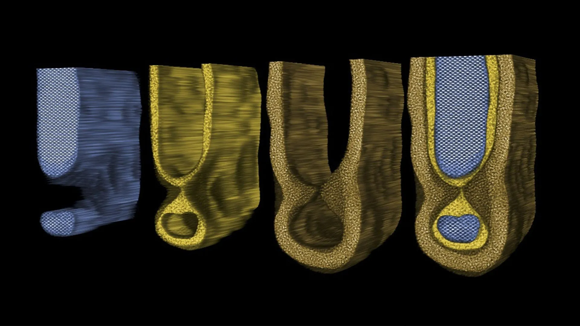
Researchers at Cornell University have achieved a groundbreaking feat, utilizing cutting-edge high-resolution 3D imaging to visualize atomic-scale defects within computer chips for the very first time. These minuscule imperfections, previously invisible and a persistent enigma for the semiconductor industry, can significantly disrupt chip performance, posing a critical challenge for the advancement of modern electronics. This revolutionary imaging technique, born from a pivotal collaboration involving Taiwan Semiconductor Manufacturing Company (TSMC) and Advanced Semiconductor Materials (ASM), promises to reshape the landscape of technology, impacting everything from the smartphones in our pockets and the cars on our roads to the vast AI data centers powering our digital world and the nascent quantum computers of the future. The landmark findings were officially published on February 23rd in the prestigious journal Nature Communications, with doctoral student Shake Karapetyan leading the charge as the study’s primary author.
"The inability to directly observe the atomic structure of these defects has been a long-standing hurdle," explained David Muller, the Samuel B. Eckert Professor of Engineering at the Cornell Duffield College of Engineering, who spearheaded this transformative project. "This new capability will serve as an indispensable characterization tool, empowering us to meticulously debug and pinpoint faults within computer chips, particularly during the crucial development stages."
The Critical Impact of Microscopic Imperfections in Semiconductor Chips
The semiconductor industry has grappled for decades with the detrimental effects of minute structural flaws. As the complexity of computer chips escalates and their constituent components shrink to the astonishing scale of individual atoms, even the slightest irregularities can profoundly influence device operation. At the heart of every computer chip lies the transistor, a minuscule component that functions as an electrical switch, meticulously controlling the flow of current. Within each transistor is a channel, a pathway that opens and closes to regulate the movement of electrons.
Muller vividly illustrates the significance of these imperfections: "Think of the transistor’s channel as a tiny pipe for electrons, analogous to how a water pipe carries water. If the internal walls of that pipe are significantly rough, it will inevitably impede the flow, slowing everything down. Therefore, accurately measuring the roughness of these walls, and identifying which sections are functioning optimally and which are compromised, has become paramount."
From Early Flat Transistors to Intricate 3D Architectures
Professor Muller’s extensive research career has been dedicated to probing the physical limitations of semiconductor technology. His tenure at Bell Labs from 1997 to 2003, the very birthplace of the transistor, was instrumental in his investigations into the ultimate limits of miniaturization for these devices. In the nascent stages of semiconductor development in the mid-20th century, transistors were arranged in planar, outward-spreading layouts, akin to suburban sprawl. However, as engineers exhausted available surface area, a paradigm shift occurred, leading to the vertical stacking of transistors. This innovative approach created incredibly complex three-dimensional structures, reminiscent of densely packed high-rise apartment buildings.
"The inherent challenge with these 3D structures," Muller elaborates, "is that they are shrinking to dimensions smaller than a virus, and in today’s advanced chips, even smaller – approaching the scale of molecules within a cell."
Modern, high-performance chips now house billions of transistors. The relentless drive towards smaller transistor sizes has made diagnosing performance issues an increasingly formidable task. Karapetyan highlights the extreme precision required: "Currently, a transistor channel can be a mere 15 to 18 atoms wide, an incredibly minuscule dimension, and these structures are extraordinarily intricate. At this scale, the precise location of every single atom matters, making characterization exceptionally challenging."
Leaps Forward in Electron Microscopy
Earlier in his career at Bell Labs, Muller collaborated with fellow scientist Glen Wilk, now Vice President of Technology at ASM. Their joint research focused on finding alternatives to silicon dioxide, the prevalent gate material at the time, which exhibited problematic current leakage as devices miniaturized. Their pioneering work significantly advanced the adoption of hafnium oxide, a material that subsequently became the industry standard for computer processors and mobile devices starting in the mid-2000s.
"The scientific papers we published on employing electron microscopes for material characterization," Muller recalls, "were meticulously studied by many in the semiconductor field. It was abundantly clear when we re-engaged with this project that the field of microscopy had undergone a monumental evolution. Back then, it felt like piloting biplanes; now, we’re operating sophisticated jets."
The "jet" Muller refers to is electron ptychography, a sophisticated computational imaging technique that leverages an electron microscope pixel array detector (EMPAD). This detector, co-developed by Muller’s research group, meticulously records intricate scattering patterns generated as electrons traverse the transistor structures. By meticulously analyzing how these scattering patterns shift between successive scan points, researchers can reconstruct remarkably detailed 3D images. The precision of this system is so exceptional that it has yielded the highest resolution images ever captured, enabling scientists to discern individual atoms with unprecedented clarity – a feat recognized by Guinness World Records.
Unveiling "Mouse Bite" Defects
More than a quarter-century after their initial collaboration, Muller and Wilk reunited, this time with crucial support from TSMC and its Corporate Analytical Laboratories group. Their collective objective was to deploy the cutting-edge EMPAD technology to examine contemporary semiconductor devices. "One can conceptualize this imaging technique as deciphering an immense puzzle," Karapetyan explains, "encompassing both the acquisition of experimental data and the subsequent computational reconstruction."
Following the meticulous collection and reconstruction of imaging data, the research team precisely mapped the positions of atoms within the transistor channels. This in-depth analysis revealed subtle irregularities, or roughness, at the interfaces of these channels. Karapetyan aptly described these imperfections as "mouse bites," a vivid analogy for their irregular, gnawed appearance. These defects are formed during the meticulously optimized growth processes employed in the manufacturing of these intricate structures. Sample devices fabricated at the Imec nanoelectronics research center provided an ideal testing ground for the advanced imaging technique.
"The fabrication of modern electronic devices involves hundreds, if not thousands, of intricate steps, including chemical etching, deposition, and thermal processing," Karapetyan notes. "Each of these steps subtly modifies the underlying structure. Previously, we relied on projected images to infer what was happening. Now, we have a direct observational tool that allows us to see the precise outcome after each individual step. This provides a far more profound understanding of how, for instance, altering the temperature during a specific process directly impacts the resulting structure."
Profound Implications for the Future of Chips and Quantum Computing
The newfound ability to directly visualize defects at the atomic level holds transformative potential for virtually every device reliant on advanced computer chips. This includes the ubiquitous smartphones and laptops that define our daily lives, as well as the massive data centers that underpin global digital infrastructure. Furthermore, this breakthrough is poised to accelerate the development of emerging technologies like quantum computing, which demands an exceptionally high degree of control over material structure.
"I believe this new tool will unlock a vast array of scientific investigations and significantly enhance our engineering control capabilities," Karapetyan concludes.
The study’s co-authors include Steven Zeltmann, a staff scientist at the Platform for the Accelerated Realization, Analysis and Discovery of Interface Materials (PARADIM), alongside Ta-Kun Chen and Vincent Hou from TSMC. Funding for this groundbreaking research was generously provided by TSMC. Essential support for the advanced microscopy facilities was contributed by CCMR and PARADIM, both of which receive funding from the National Science Foundation.