At the heart of this innovation lies the chip’s ability to perform convolution operations, a fundamental building block of machine learning algorithms. These operations are crucial for AI systems to effectively discern intricate patterns and features within vast datasets, particularly in image, video, and text analysis. Traditionally, these convolutions require immense processing power, translating directly into substantial energy consumption. The University of Florida team’s ingenious solution involves the direct integration of optical components onto a standard silicon chip. This fusion allows for convolutions to be executed using laser light and precisely engineered microscopic lenses. The result is a dramatic reduction in energy usage, often by orders of magnitude, and a significant acceleration of processing speeds.
"Performing a key machine learning computation at near zero energy is a leap forward for future AI systems," stated study leader Volker J. Sorger, the esteemed Rhines Endowed Professor in Semiconductor Photonics at the University of Florida. He emphasized the critical importance of this breakthrough for the continued scaling and advancement of AI capabilities in the coming years. The implications for energy-constrained environments and the broader goal of sustainable technology are profound. Imagine AI applications that can run for extended periods on minimal power, enabling widespread deployment in remote locations, on battery-powered devices, or within data centers striving for carbon neutrality.
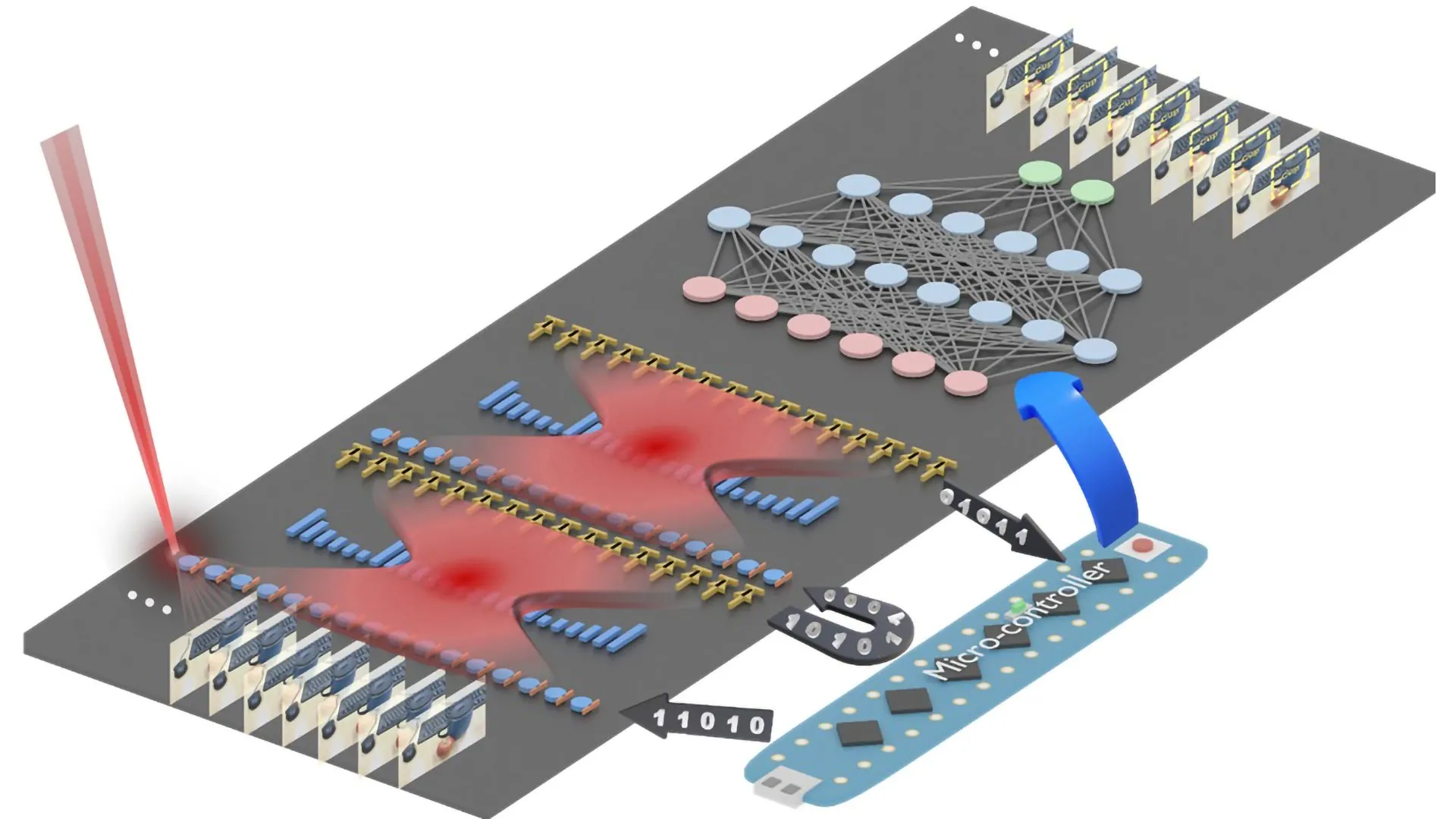
In rigorous testing, the prototype chip demonstrated remarkable efficacy. It successfully classified handwritten digits with an accuracy rate of approximately 98 percent, a performance level directly comparable to that of conventional electronic chips. This parity in accuracy, coupled with the vastly reduced energy footprint, underscores the practical viability of this optical approach. The chip’s optical prowess is facilitated by two sets of miniature Fresnel lenses. These lenses, essentially flat and ultrathin versions of the large, multifaceted lenses found in lighthouses, are fabricated using established semiconductor manufacturing techniques, ensuring scalability and potential for mass production. The lenses themselves are incredibly small, with dimensions narrower than a human hair, and are directly etched onto the chip’s surface.
The process by which the chip performs a convolution is elegantly orchestrated. Machine learning data is first converted into a beam of laser light upon entering the chip. This light then traverses through the precisely shaped Fresnel lenses. These lenses act as optical processors, performing the complex mathematical transformations inherent in the convolution operation. Once the optical computation is complete, the resulting light signal is converted back into a digital format, thereby finalizing the AI task. This seamless transition between optical and electronic domains is a testament to the sophisticated design and engineering involved.
Hangbo Yang, a research associate professor within Sorger’s group at UF and a co-author of the study, highlighted the novelty of their achievement. "This is the first time anyone has put this type of optical computation on a chip and applied it to an AI neural network," Yang remarked, underscoring the pioneering nature of their work. This achievement opens up entirely new avenues for AI hardware design, moving beyond the limitations of purely electronic components.
Further enhancing the chip’s capabilities, the research team also showcased its ability to process multiple data streams concurrently. This is achieved through the ingenious use of lasers emitting different colors of light. This technique, known as wavelength multiplexing, allows for a significant increase in data throughput without a proportional increase in energy expenditure. "We can have multiple wavelengths, or colors, of light passing through the lens at the same time," Yang explained. "That’s a key advantage of photonics." This parallel processing capability is crucial for handling the ever-increasing volumes of data that AI systems are tasked with analyzing.
The development of this revolutionary chip was not an isolated endeavor but a collaborative effort involving several leading institutions. The research was conducted in close partnership with the Florida Semiconductor Institute, the University of California, Los Angeles (UCLA), and George Washington University. This multidisciplinary collaboration brought together expertise from photonics, semiconductor engineering, and artificial intelligence, fostering a holistic approach to the challenge. Sorger also pointed to the existing landscape of AI chip manufacturing, noting that industry giants like NVIDIA already incorporate optical elements into certain aspects of their AI systems. This existing integration could significantly streamline the adoption and implementation of this new optical AI technology.
Looking ahead, Sorger expressed a strong conviction about the future trajectory of AI hardware. "In the near future, chip-based optics will become a key part of every AI chip we use daily," he predicted. "And optical AI computing is next." This statement encapsulates the transformative potential of their research, suggesting that the integration of optics into AI chips will not be a niche development but a fundamental shift that will redefine the performance, efficiency, and sustainability of artificial intelligence for years to come. The promise of AI that is not only more powerful but also significantly more environmentally responsible is now closer than ever, thanks to the light-powered innovation emerging from the University of Florida. This breakthrough has the potential to democratize AI, making it more accessible and sustainable for a wider range of applications and industries, from edge computing devices to massive-scale data centers, all while contributing to a greener technological future. The implications for reducing the carbon footprint of the digital world are immense, paving the way for a new era of intelligent technologies that are both powerful and planet-friendly.