This revolutionary imaging technique, a testament to collaborative innovation, was meticulously developed through a synergistic partnership involving global leaders in semiconductor manufacturing and materials science: Taiwan Semiconductor Manufacturing Company (TSMC) and Advanced Semiconductor Materials (ASM). The profound implications of this discovery extend across a vast spectrum of technological domains, as computer chips form the very bedrock of the devices that define our modern lives. From the ubiquitous smartphones we carry in our pockets and the increasingly sophisticated vehicles that transport us, to the colossal AI data centers that power artificial intelligence and the nascent yet promising realm of quantum computers, the ability to understand and mitigate atomic-level flaws holds the key to unlocking unprecedented levels of performance, efficiency, and reliability.
The seminal findings of this research were formally disseminated to the scientific community on February 23rd, published in the esteemed journal Nature Communications. The intellectual engine driving this remarkable achievement was spearheaded by doctoral student Shake Karapetyan, who served as the lead author of the study, meticulously guiding the research to its successful conclusion.
"Since there’s really no other way you can see the atomic structure of these defects, this is going to be a really important characterization tool for debugging and fault-finding in computer chips, especially at the development stage," articulated David Muller, the Samuel B. Eckert Professor of Engineering at the Cornell Duffield College of Engineering, who masterminded the project. His words underscore the transformative potential of this new methodology, positioning it as an indispensable asset for engineers and scientists striving to perfect the intricate architecture of future electronic components.
The Critical Significance of Microscopic Defects in Semiconductor Chips
The semiconductor industry has grappled for decades with the challenge posed by exceedingly small structural flaws. As the complexity of computer chips has escalated exponentially, and their constituent components have been miniaturized to the astonishing scale of individual atoms, even the most minute irregularities have begun to exert a disproportionate influence on device operation. These seemingly insignificant imperfections can act as roadblocks to the smooth flow of electrons, introduce unwanted resistance, or even create short circuits, thereby degrading performance, reducing lifespan, and leading to outright failures.
At the very heart of every computer chip lies the transistor, a marvel of miniaturization that functions as an electronic switch. This minuscule component is responsible for precisely controlling the movement of electrical current, acting as a gatekeeper that can either allow or block the passage of electrons. Each transistor incorporates a channel, a carefully designed pathway through which electrons travel. The ability of this channel to open and close efficiently and reliably is fundamental to the transistor’s function and, by extension, the overall performance of the chip.
"The transistor is like a little pipe for electrons instead of water," Professor Muller elucidated, drawing a relatable analogy. "You can imagine, if the walls of the pipe are very rough, it’s going to slow things down. And so measuring how rough the walls are and which walls are good and which walls are bad is now even more important." This analogy vividly illustrates how even subtle imperfections in the atomic structure of the transistor channel can impede the flow of electrons, akin to a rough pipe hindering water flow, leading to reduced speed and efficiency.
Evolution from Early Transistors to Sophisticated 3D Chip Architectures
Professor Muller’s distinguished career has been deeply intertwined with the relentless pursuit of understanding and pushing the physical limits of semiconductor technology. His foundational work dates back to his tenure at Bell Labs from 1997 to 2003, a period marked by intensive research and development aimed at uncovering the ultimate achievable miniaturization of transistors. It was at Bell Labs, the very birthplace of the transistor, that he began to probe the fundamental constraints on how small these essential components could become.
In the nascent days of transistors, during the mid-20th century, they were predominantly laid out on chips in flat, two-dimensional configurations. This arrangement was akin to the outward expansion of suburban communities, spreading across available surface area. However, as engineers pushed the boundaries of miniaturization, they eventually encountered the physical limitations of two-dimensional space. This challenge spurred a paradigm shift in chip design, leading to the revolutionary concept of stacking transistors vertically. This innovative approach transformed the landscape of chip architecture, giving rise to complex three-dimensional structures that bear a striking resemblance to the towering edifices of modern high-rise apartment buildings.
"The problem is these 3D structures are smaller than the size of a virus. And these days, it’s a lot smaller. It’s more like a molecule-in-the-cell kind of scale," Professor Muller emphasized, highlighting the extreme miniaturization involved. This dramatic reduction in scale means that the tolerances for error are vanishingly small, making even the slightest atomic-level deviation a significant concern.
Today, a single advanced computer chip can house an astonishingly dense array of billions of transistors. As their physical dimensions have continued to shrink, the task of diagnosing and rectifying performance issues has become increasingly formidable. The intricate interplay of billions of atomic-scale components means that pinpointing the root cause of a malfunction can feel like searching for a needle in an impossibly vast haystack.
"These days, a transistor channel can be only about 15 to 18 atoms wide, which is super, super tiny, and they’re extremely intricate," explained Shake Karapetyan, reinforcing the scale of the challenge. "At this point, it matters where every atom is, and it’s really hard to characterize." The precision required at this level is so profound that the exact positioning of each individual atom becomes a critical factor in determining the transistor’s functionality.
Leaps Forward in Electron Microscopy Capabilities
The genesis of this groundbreaking research can be traced back to an earlier collaboration between Professor Muller and his former colleague, Glen Wilk, who was a scientist at Bell Labs during the same period and is now a vice president of technology at ASM. Their joint efforts focused on identifying and implementing alternative materials to replace silicon dioxide, which was the dominant gate dielectric material at the time. Silicon dioxide, while effective, suffered from excessive current leakage when devices were scaled down to very small dimensions, posing a significant obstacle to further miniaturization. Their pioneering research played a crucial role in advancing the adoption of hafnium oxide, a material that subsequently became the industry standard for gate dielectrics in computer processors and mobile devices, beginning in the mid-2000s.
"The papers we published on how to use electron microscopes to characterize these materials, I can tell you, a lot of the semiconductor folks had read those very, very carefully," Professor Muller remarked, underscoring the significant impact of their earlier work on the broader semiconductor industry. "When we got back into this project, that was very clear. And the microscopy has gone a very long way. Back then, it was like flying biplanes. And now you’ve got jets." This powerful analogy effectively conveys the dramatic advancement in electron microscopy technology, from rudimentary capabilities to the sophisticated, high-performance tools available today.
The "jet" Professor Muller refers to is a cutting-edge computational imaging technique known as electron ptychography. This sophisticated method relies on a specialized detector called an electron microscope pixel array detector (EMPAD), a technology that was co-developed by Professor Muller’s own research group. The EMPAD is designed to meticulously record the intricate diffraction patterns generated as a beam of electrons traverses the complex three-dimensional structures of the transistors.
By precisely analyzing and comparing the subtle shifts in these scattering patterns across different scan points, researchers are able to computationally reconstruct extraordinarily detailed images of the atomic structure. The system’s remarkable precision has enabled the capture of images with the highest resolution ever achieved, allowing scientists to visualize individual atoms with an unprecedented level of clarity. This extraordinary capability has even been recognized by Guinness World Records, solidifying its status as a landmark achievement in scientific imaging.
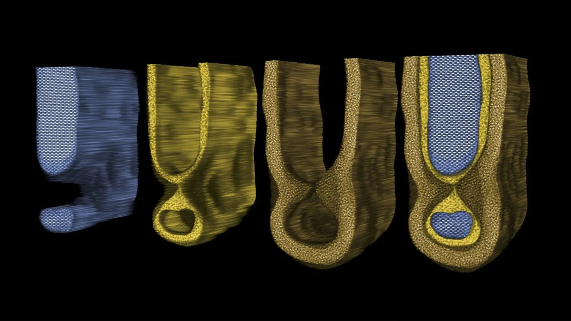
The Discovery of "Mouse Bite" Defects and Their Significance
More than a quarter of a century after their initial collaboration, Professor Muller and Glen Wilk reunited, this time with the crucial support of TSMC and its dedicated Corporate Analytical Laboratories group. Their collective objective was to apply the advanced EMPAD technology to the examination of modern semiconductor devices, pushing the boundaries of what was previously possible in chip analysis.
"You can think of this imaging technique like solving a massive puzzle, both in terms of taking the experimental data and doing the computational reconstruction," explained Shake Karapetyan, illustrating the complex yet rewarding nature of the research process. The reconstruction of the 3D atomic structure from the collected diffraction data is indeed akin to assembling an incredibly intricate jigsaw puzzle, requiring sophisticated algorithms and computational power.
Following the meticulous collection and computational reconstruction of the imaging data, the research team embarked on a detailed analysis of the atomic positions within the critical transistor channels. This in-depth examination led to a pivotal discovery: the identification of subtle roughness along the interfaces of these channels. Karapetyan aptly described these irregular patterns as "mouse bites," a vivid descriptor for the small, irregular indentations observed at the atomic scale.
These "mouse bite" defects were found to form during the highly optimized growth processes employed in the manufacturing of these advanced semiconductor structures. To rigorously test and validate their imaging technique, the researchers utilized sample devices fabricated at Imec, a world-leading nanoelectronics research center, which provided an ideal platform for their experiments.
"Fabrication of modern devices takes hundreds, if not thousands, of steps of chemical etching and deposition and heating, and then every single step does something to your structure," Karapetyan noted, emphasizing the cumulative impact of each manufacturing step. "Before you used to look at projective images to try to figure out what was really going on. Now you have a direct probe to actually see after every single step and have a better grasp of, oh, I put the temperature this high, and then this is what it looks like." This highlights the immense advantage of real-time, atomic-level visualization; instead of inferring structural changes from indirect measurements, scientists can now directly observe the consequences of each manufacturing step, allowing for immediate adjustments and optimization.
Far-Reaching Implications for Future Chip Development and Quantum Computing
The newfound ability to directly observe and quantify atomic-level defects holds profound implications for a vast array of technologies that rely on sophisticated computer chips. This includes the ubiquitous smartphones and laptops that form the backbone of our personal and professional lives, as well as the massive data centers that power cloud computing and artificial intelligence. Furthermore, this breakthrough is poised to accelerate the development of nascent and highly promising technologies, such as quantum computers. Quantum computing, in particular, demands an extraordinarily precise and controlled atomic structure of materials, making the ability to identify and rectify atomic-scale imperfections absolutely critical.
"I think there’s a lot more science we can do now, and a lot more engineering control, having this tool," Karapetyan expressed with optimism, underscoring the expansive potential for future research and technological advancement. The ability to see, understand, and manipulate at the atomic level opens up entirely new avenues for scientific discovery and engineering innovation.
The groundbreaking study was further enriched by the contributions of several other esteemed researchers. Co-authors of the publication include Steven Zeltmann, a staff scientist at the Platform for the Accelerated Realization, Analysis and Discovery of Interface Materials (PARADIM), along with Ta-Kun Chen and Vincent Hou from TSMC.
The research received vital financial backing from TSMC, a testament to the industry’s recognition of the significance of this work. Crucial support for the advanced microscopy facilities was generously provided by the Cornell Center for Materials Research (CCMR) and PARADIM, both of which receive funding from the National Science Foundation, further highlighting the collaborative and publicly supported nature of this scientific endeavor.