Engineers have taken a major step toward producing the smallest earthquakes ever created, shrinking seismic-style vibrations down to the scale of a microchip. This groundbreaking development centers on a novel device dubbed a surface acoustic wave (SAW) phonon laser, a technology poised to revolutionize the capabilities of chips found in smartphones and a vast array of other wireless electronics, promising devices that are not only more compact but also boast enhanced speed and superior energy efficiency. The pioneering research was spearheaded by Matt Eichenfield, an esteemed incoming faculty member at the University of Colorado Boulder, in close collaboration with a distinguished team of scientists from the University of Arizona and Sandia National Laboratories. Their seminal findings, detailing this significant technological leap, were officially published on January 14th in the prestigious scientific journal Nature.
At the heart of this innovation lies the manipulation of surface acoustic waves, more commonly referred to as SAWs. These waves, while sharing a conceptual similarity with sound waves, exhibit a crucial distinction: rather than propagating through the bulk of a material or through the air, they are confined to travel exclusively along the surface of a solid. The raw power of SAWs is dramatically illustrated by large-scale seismic events, where they manifest as colossal ripples across the Earth’s crust, capable of inducing widespread destruction and societal disruption. However, on a vastly diminished scale, SAWs are already indispensable components underpinning many of the sophisticated technologies that define modern life. "SAWs devices are critical to the many of the world’s most important technologies," emphatically stated Eichenfield, who holds the distinguished Gustafson Endowed Chair in Quantum Engineering at CU Boulder and served as the senior author of this groundbreaking study. He further elaborated on their ubiquity, noting, "They’re in all modern cell phones, key fobs, garage door openers, most GPS receivers, many radar systems and more."
The integral role of SAWs in powering smartphones is already well-established. Within the intricate architecture of a smartphone, these surface acoustic waves perform the vital function of highly precise filters. When radio signals arrive from a cellular tower, they are initially transmuted into minute mechanical vibrations. This conversion is instrumental in enabling the device’s internal chips to meticulously distinguish between valuable incoming signals and disruptive interference or ambient background noise. Once the signal has been effectively purified, these cleaned vibrations are then reconverted back into radio waves, facilitating seamless communication.
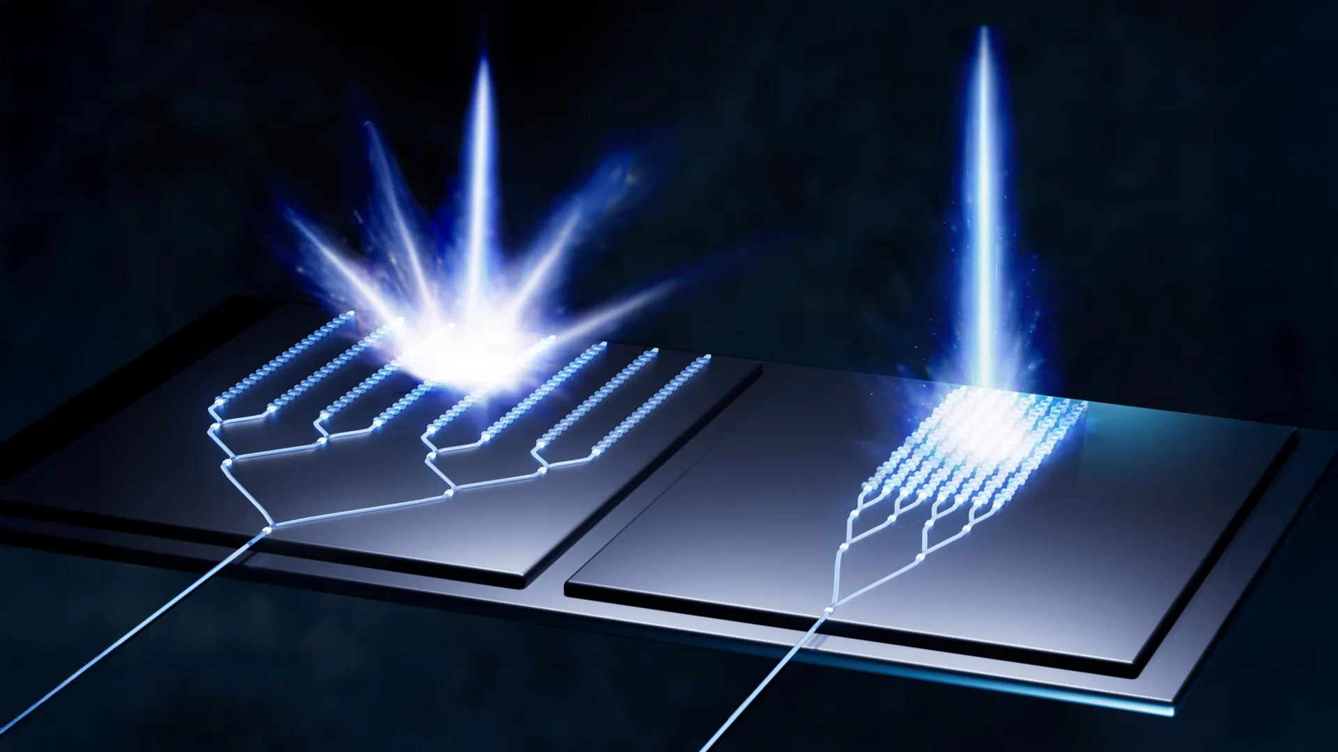
The current study, however, introduces a revolutionary new paradigm for generating these essential surface waves. Eichenfield and his collaborators have unveiled a novel method employing what they term a "phonon laser." In stark contrast to the familiar operation of a conventional laser pointer, which emits focused beams of light, this innovative device is engineered to produce precisely controlled mechanical vibrations. "Think of it almost like the waves from an earthquake, only on the surface of a small chip," explained Alexander Wendt, a graduate student at the University of Arizona and the lead author of this pivotal research. A significant advantage of this new design lies in its potential for miniaturization and integration. Most existing SAW systems necessitate the use of two distinct chips and an external power source. The innovative approach developed by the research team consolidates all these functionalities into a single, unified chip. Furthermore, it holds the promise of operating efficiently on a simple battery, while simultaneously achieving significantly higher operating frequencies than current technologies.
To truly grasp the essence of this new device, it is beneficial to first understand the fundamental principles behind conventional lasers. Many commonly encountered lasers, such as diode lasers, operate by generating light through a process of repeated reflection between two miniature mirrors embedded within a semiconductor chip. As photons of light bounce back and forth within this resonant cavity, they interact with energized atoms, which, when stimulated, release additional photons, thereby amplifying and strengthening the emitted light beam. Eichenfield drew a direct parallel to this established technology, stating, "Diode lasers are the cornerstone of most optical technologies because they can be operated with just a battery or simple voltage source, rather than needing more light to create the laser like a lot of previous kinds of lasers. We wanted to make an analog of that kind of laser but for SAWs."
In pursuit of this ambitious goal, the research team meticulously constructed a specialized bar-shaped device, measuring approximately half a millimeter in length. This compact structure is composed of a carefully engineered stack of distinct materials, each contributing unique properties to the overall functionality. At the base of this layered assembly lies silicon, the ubiquitous semiconductor material that forms the bedrock of the vast majority of modern computer chips. Positioned directly above the silicon is a meticulously thin layer of lithium niobate, a material renowned for its piezoelectric properties. Piezoelectricity means that when lithium niobate is subjected to mechanical stress or vibration, it generates oscillating electric fields. Conversely, applying an electric field to lithium niobate can induce mechanical vibrations. The uppermost layer of this intricate structure is an exceptionally thin sheet of indium gallium arsenide. This material possesses remarkable electronic characteristics, notably its ability to accelerate electrons to extremely high velocities even under the influence of relatively weak electric fields. The synergistic integration of these layered materials creates a unique environment where vibrations propagating along the surface of the lithium niobate layer can directly interact with these fast-moving electrons within the indium gallium arsenide.
The researchers vividly describe the operational mechanism of their phonon laser by drawing an analogy to a wave pool. When an electric current is introduced and flows through the indium gallium arsenide layer, it instigates the formation of surface waves within the lithium niobate layer. These nascent waves then propagate forward, encounter a specially designed reflector, and subsequently rebound, traveling backward. This dynamic of forward and backward propagation is strikingly similar to the principle of light reflecting between mirrors in a conventional laser. Each forward journey of the wave imbues it with additional energy, effectively strengthening it. Conversely, each backward pass, as it moves against the direction of amplification, results in a significant loss of energy. "It loses almost 99% of its power when it’s moving backward, so we designed it to get a substantial amount of gain moving forward to beat that," commented Wendt, highlighting the critical design challenge of overcoming these inherent losses. After undergoing numerous such iterative passes, the vibrations progressively amplify to a sufficient intensity. At this juncture, a portion of the generated wave energy is strategically allowed to escape from one edge of the device, much like how a laser beam eventually exits its optical cavity.
The practical implications of this phonon laser technology are profound, particularly in its ability to generate surface acoustic waves at exceptionally high frequencies. Using their innovative approach, the research team successfully generated SAWs vibrating at approximately 1 gigahertz, which translates to an astonishing one billion oscillations per second. The researchers are confident that with further refinement of their design, this frequency could be pushed into the tens or even hundreds of gigahertz. This represents a significant advancement over traditional SAW devices, which typically reach their operational limit around 4 gigahertz, making the new system demonstrably faster.
Eichenfield expressed optimism about the transformative potential of this breakthrough, stating that the advance could pave the way for the development of wireless devices that are not only more compact but also possess greater processing power and exhibit significantly improved energy efficiency. He elaborated on the current inefficiencies in modern smartphones, where multiple specialized chips are repeatedly tasked with the conversion of radio waves into SAWs and vice versa for every communication event, whether it be sending messages, making calls, or browsing the internet. The ultimate ambition of the research team is to drastically simplify this process by developing a single, integrated chip capable of handling all essential signal processing functions using the inherent capabilities of surface acoustic waves. "This phonon laser was the last domino standing that we needed to knock down," Eichenfield declared, underscoring the significance of their achievement. "Now we can literally make every component that you need for a radio on one chip using the same kind of technology." This paradigm shift promises a future of more integrated, powerful, and energy-conscious personal electronics.