
 Imroatul Nasiyah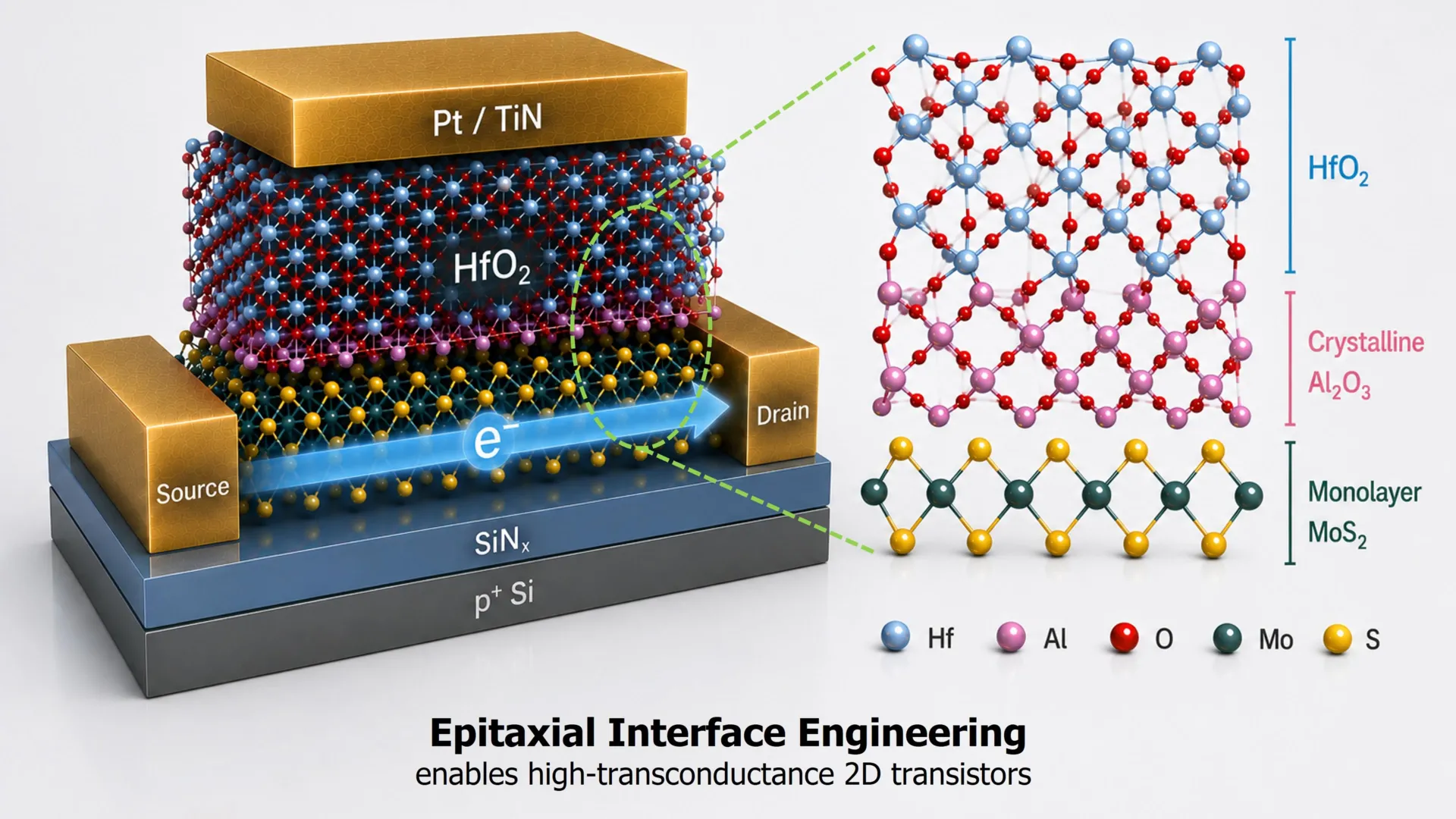
At the heart of a functional transistor lies the gate dielectric, an ultra-thin insulating layer crucial for controlling the flow of electrons. As transistors continue their relentless miniaturization, reducing the thickness of this dielectric layer becomes paramount for enhancing electrical control. The challenge arises when attempting to integrate these ultra-thin dielectrics with atomically thin semiconductors. Such an integration often disrupts the delicate interface between the materials, leading to electron scattering and diminishing the very performance gains researchers strive to achieve. This fundamental conflict has historically forced engineers to make a difficult choice: prioritize enhanced gate control or preserve the mobility of charge carriers within the device. Achieving both simultaneously has been an elusive goal, a trade-off that has long constrained the advancement of 2D transistors.
However, a paradigm shift in approach has emerged from researchers at National Yang Ming Chiao Tung University (NYCU), in collaboration with TSMC Corporate Research. Their groundbreaking work, detailed in the prestigious journal Nature Electronics, reorients the focus from discovering new semiconductor materials to meticulously engineering the interface itself. By precisely controlling the atomic boundary between the semiconductor and its insulating layer, they have demonstrated the feasibility of creating extremely thin dielectrics while maintaining robust electrical performance. This novel strategy bypasses the need for entirely new semiconductor compositions, instead concentrating on the critical, few-atom-thick region where materials converge.
Professor Wen-Hao Chang, the study’s corresponding author from NYCU, highlighted the significance of this shift in perspective. "For many years, efforts to improve atomically thin transistors have largely focused on discovering better semiconductor materials," he stated. "Our research shows that the atomic interface between materials can be just as important. By engineering that boundary, we were able to reduce one of the fundamental trade-offs that has limited two-dimensional transistors for many years." This insight underscores a nascent understanding that the seemingly passive interfaces between materials are, in fact, active participants in device functionality.
The importance of this atomic interface is deeply rooted in the continuous drive for miniaturization in modern chip development. The gate dielectric, which serves as the electrical separator between the gate electrode and the transistor channel, is a critical component in this miniaturization process. While decades of refinement have enabled the production of highly effective dielectric materials for silicon-based transistors, atomically thin semiconductors present a unique set of challenges. Their surfaces, lacking the "dangling bonds" found in bulk materials, make it difficult to deposit an extremely thin dielectric film uniformly and without defects.
Standard deposition techniques can inadvertently introduce gaps, create interfacial defects, and induce electrical disorder. These imperfections can significantly impede the movement of charge carriers, thereby degrading transistor performance. Researchers globally have explored various solutions, including novel dielectric materials, molecular seed layers, and alternative deposition methods for oxides. While these efforts have yielded incremental improvements, achieving a simultaneous trifecta of low equivalent oxide thickness, strong electrostatic control, and high carrier mobility has remained a formidable challenge, particularly in the context of wafer-scale Chemical Vapor Deposition (CVD)-grown monolayer MoS2, a promising 2D semiconductor.
The NYCU team’s innovative solution lies in their redesign of the interface connecting the semiconductor and the gate dielectric, rather than altering either material itself. Their approach begins with the deposition of an ultrathin epitaxial aluminum layer directly onto monolayer molybdenum disulfide (MoS2). This aluminum layer is then carefully oxidized, forming an aluminum oxide layer approximately 0.42 nanometers thick. Subsequently, a high-k hafnium oxide gate dielectric is added. This engineered interface, despite its minuscule thickness of just a fraction of a nanometer, performs two crucial functions.
Firstly, it establishes a smooth and continuous surface, facilitating the uniform growth of the hafnium oxide dielectric over the MoS2. This uniformity is essential for preventing defects and ensuring consistent dielectric properties. Secondly, this ultrathin aluminum oxide layer acts as an atomic buffer, effectively mitigating unwanted electrical interactions between the dielectric and the semiconductor. This buffering action is vital for preserving the unimpeded flow of electrons through the transistor channel, a critical factor for high-speed operation and energy efficiency. In essence, the interface transcends its traditional role of mere separation, becoming an integral functional component that optimizes the synergistic interaction between the materials.
Leveraging this novel interface design, the researchers successfully fabricated short-channel top-gate transistors using CVD-grown monolayer MoS2. These devices exhibited an equivalent oxide thickness of approximately one nanometer. Rigorous testing revealed exceptionally low leakage current, minimal hysteresis (a measure of device stability), and a maximum transconductance of 0.45 mS μm-1 in transistors with channel lengths around 100 nanometers. Crucially, these transistors achieved a combination of desirable attributes that have historically been difficult to attain in atomically thin devices: ultra-thin dielectric scaling, potent electrostatic control, and sustained carrier transport. The fact that the researchers utilized CVD-grown monolayer MoS2, a method more amenable to large-scale manufacturing than mechanically exfoliated flakes, significantly bolsters the technology’s prospects for eventual wafer-scale production.
These findings herald a broader conceptual shift in how semiconductor researchers approach transistor design. For decades, the focus has been primarily on the discovery of superior semiconductor materials or the relentless shrinking of device dimensions. However, as transistor components approach atomic scales, the interfaces that delineate different materials are increasingly recognized as critical determinants of device performance. These interfaces, though only a few atoms thick, exert a profound influence on the collaborative functionality of the constituent materials. The current research adds substantial weight to the growing body of evidence suggesting that the precise control of these atomic interfaces could become as vital as the development of entirely new semiconductor materials.
Professor Tsung-En Lee, another corresponding author of the study, emphasized this evolving understanding: "When transistor components become only a few atomic layers thick, the interface is no longer simply the boundary between materials; it becomes an active part of the device," he explained. "Learning to engineer these interfaces with atomic precision opens new opportunities for designing future semiconductor devices that would be difficult to achieve by changing individual materials alone." This perspective suggests a future where the "art" of semiconductor design involves a deep understanding and manipulation of the nanoscale architecture at material junctions.
As the semiconductor industry actively seeks pathways to transcend the limitations of traditional silicon scaling, atomically thin materials are garnering significant attention for their potential in next-generation low-power logic and advanced electronic systems. While further optimization of the fabrication process is necessary for large-scale manufacturing, the NYCU team’s interface engineering method represents a significant stride toward realizing practical 2D electronics. The implications of these findings extend beyond the immediate advancement of transistors; they point towards a future where innovation in semiconductor technology will be driven not only by the discovery of novel materials but also by the mastery of controlling the atomic boundaries that bind them. As transistors continue their journey toward the dimensions of individual atoms, these interfaces are poised to emerge as some of the most critical, and indeed, most exciting components of future electronic devices.