For the first time, researchers at Cornell University have harnessed advanced 3D imaging techniques to precisely pinpoint atomic-scale defects within the intricate architecture of computer chips. This groundbreaking discovery, born from a significant collaboration with industry giants Taiwan Semiconductor Manufacturing Company (TSMC) and Advanced Semiconductor Materials (ASM), marks a pivotal moment for the entire field of modern electronics. These minute imperfections, previously elusive and a persistent impediment to optimal chip performance, have now been brought into sharp focus, promising to accelerate innovation across a vast spectrum of technological domains, from the smartphones in our pockets and the vehicles on our roads to the colossal data centers powering artificial intelligence and the nascent frontiers of quantum computing. The findings, meticulously detailed in the prestigious journal Nature Communications on February 23rd, were spearheaded by doctoral student Shake Karapetyan, with Professor David Muller of the Cornell Duffield College of Engineering leading the transformative project.
Professor Muller, the Samuel B. Eckert Professor of Engineering, articulated the profound significance of this breakthrough: "Since there’s really no other way you can see the atomic structure of these defects, this is going to be a really important characterization tool for debugging and fault-finding in computer chips, especially at the development stage." This new capability provides an indispensable diagnostic tool, allowing engineers to understand and rectify issues at their most fundamental level.
The semiconductor industry has long grappled with the challenges posed by minuscule structural flaws. As computer chips have evolved into increasingly complex systems, with their constituent components shrinking to the scale of individual atoms, even the slightest irregularity can profoundly impact device functionality. At the heart of every computer chip lies the transistor, a fundamental building block that acts as an electronic switch, controlling the flow of electrical current. Each transistor incorporates a channel that opens and closes, meticulously regulating the passage of electrons. Professor Muller vividly illustrated this concept: "The transistor is like a little pipe for electrons instead of water. You can imagine, if the walls of the pipe are very rough, it’s going to slow things down. And so measuring how rough the walls are and which walls are good and which walls are bad is now even more important." This analogy underscores the critical need for precision at the atomic level.
Professor Muller’s distinguished career has been dedicated to exploring the physical limitations of semiconductor technology. His tenure at Bell Labs from 1997 to 2003 involved pioneering research into the ultimate miniaturization of transistors, the very devices invented at that institution. In the early days of transistors, their arrangement on chips was largely two-dimensional, spreading outwards horizontally. However, as engineers exhausted available surface area, a paradigm shift occurred, leading to the development of vertically stacked, three-dimensional chip structures that bear a resemblance to towering apartment buildings. "The problem is these 3D structures are smaller than the size of a virus. And these days, it’s a lot smaller. It’s more like a molecule-in-the-cell kind of scale," Muller noted, highlighting the extraordinary miniaturization achieved.
Today’s advanced chips can house billions of transistors, and as their dimensions continue to contract, diagnosing performance issues has become an increasingly arduous task. Karapetyan elaborated on this challenge: "These days, a transistor channel can be only about 15 to 18 atoms wide, which is super, super tiny, and they’re extremely intricate. At this point, it matters where every atom is, and it’s really hard to characterize." This level of precision demanded by modern electronics necessitates tools capable of resolving structures at the atomic scale.
The advancements in electron microscopy that underpin this discovery have a rich history. Earlier in his career at Bell Labs, Professor Muller collaborated with Glen Wilk, now Vice President of Technology at ASM. Their joint research focused on finding alternatives to silicon dioxide, then the prevalent gate material, which suffered from excessive current leakage in miniaturized devices. Their work contributed to the widespread adoption of hafnium oxide, which subsequently became the standard gate dielectric material in processors for computers and mobile devices. Muller reflected on the impact of their past work: "The papers we published on how to use electron microscopes to characterize these materials, I can tell you, a lot of the semiconductor folks had read those very, very carefully. When we got back into this project, that was very clear. And the microscopy has gone a very long way. Back then, it was like flying biplanes. And now you’ve got jets." This evocative comparison highlights the dramatic leap in technological capability.
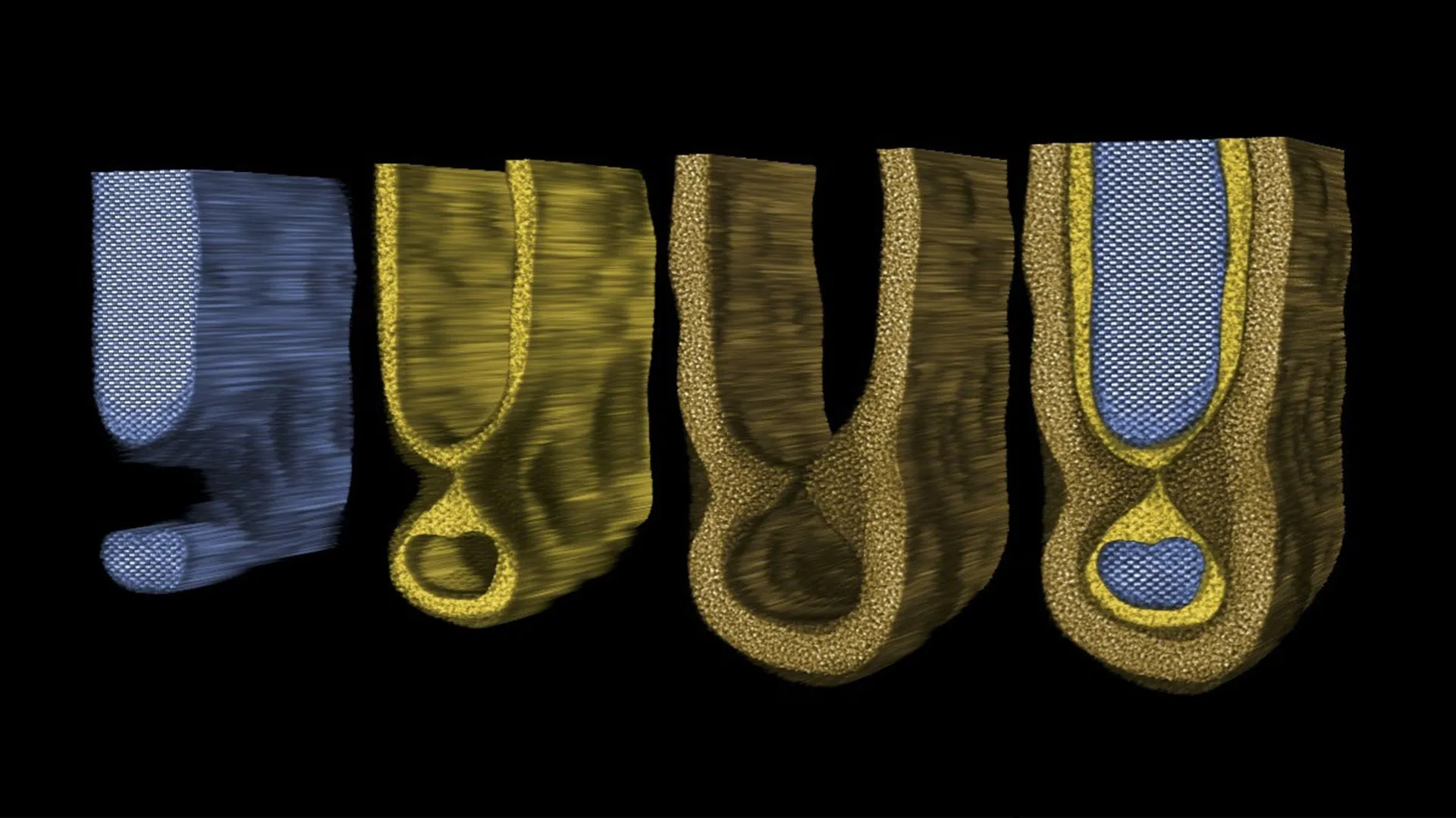
The "jet" Muller refers to is electron ptychography, a sophisticated computational imaging technique that leverages the electron pixel array detector (EMPAD). This detector, co-developed by Muller’s research group, captures intricate scattering patterns generated as electrons traverse the transistor structures. By meticulously analyzing the subtle variations in these scattering patterns across different scan points, researchers can reconstruct highly detailed three-dimensional images. The precision of this system has yielded the highest resolution images ever recorded, enabling scientists to visualize individual atoms with unprecedented clarity, a feat even recognized by Guinness World Records.
The renewed collaboration between Muller and Wilk, joined by the crucial support of TSMC and its Corporate Analytical Laboratories, aimed to apply this cutting-edge EMPAD technology to contemporary semiconductor devices. Karapetyan likened the imaging process to solving a complex puzzle: "You can think of this imaging technique like solving a massive puzzle, both in terms of taking the experimental data and doing the computational reconstruction."
Following the acquisition and reconstruction of imaging data, the researchers meticulously tracked the positions of atoms within the transistor channels. This rigorous analysis revealed subtle irregularities along the interfaces of these channels, which Karapetyan aptly described as "mouse bites." These defects emerged during the optimized manufacturing processes employed for creating these intricate structures. The nanoelectronics research center Imec provided an ideal platform for testing this novel imaging technique through its meticulously fabricated sample devices. Karapetyan further explained the implications for manufacturing: "Fabrication of modern devices takes hundreds, if not thousands, of steps of chemical etching and deposition and heating, and then every single step does something to your structure. Before you used to look at projective images to try to figure out what was really going on. Now you have a direct probe to actually see after every single step and have a better grasp of, oh, I put the temperature this high, and then this is what it looks like." This direct visual feedback loop promises to dramatically improve manufacturing yields and device reliability.
The ability to directly observe defects at the atomic level has far-reaching implications for a vast array of technologies reliant on advanced computer chips. This includes not only consumer electronics like smartphones and laptops but also the massive data centers that form the backbone of the digital economy. Furthermore, this breakthrough holds immense promise for the development of nascent technologies such as quantum computers, which demand an exceptionally high degree of control over material structures. "I think there’s a lot more science we can do now, and a lot more engineering control, having this tool," Karapetyan enthused, underscoring the transformative potential of this new diagnostic capability.
The research team also acknowledged the contributions of co-authors Steven Zeltmann from PARADIM and Ta-Kun Chen and Vincent Hou from TSMC. The study received funding from TSMC, with support for the microscopy facilities provided by CCMR and PARADIM, both of which are funded by the National Science Foundation, underscoring the collaborative and publicly supported nature of this significant scientific endeavor. This advancement represents a monumental step forward in our ability to understand, control, and ultimately optimize the performance of the electronic devices that shape our modern world.