Artificial intelligence (AI) systems have rapidly become indispensable pillars of modern technology, permeating every facet of our digital lives, from the sophisticated algorithms that power facial recognition and real-time language translation to the complex decision-making processes in autonomous vehicles and advanced scientific research. However, this pervasive integration comes with a significant and growing environmental cost. As AI models balloon in complexity and computational demands, their appetite for electricity escalates dramatically, presenting formidable challenges to energy efficiency, environmental sustainability, and the long-term scalability of AI itself. In a groundbreaking development that promises to revolutionize the energy landscape of artificial intelligence, researchers at the University of Florida have engineered a novel chip that harnesses the power of light to perform one of AI’s most energy-intensive tasks, potentially achieving an astonishing 100-fold increase in efficiency. This pioneering research, detailed in the prestigious journal Advanced Photonics, marks a pivotal moment in the quest for greener and more powerful AI.
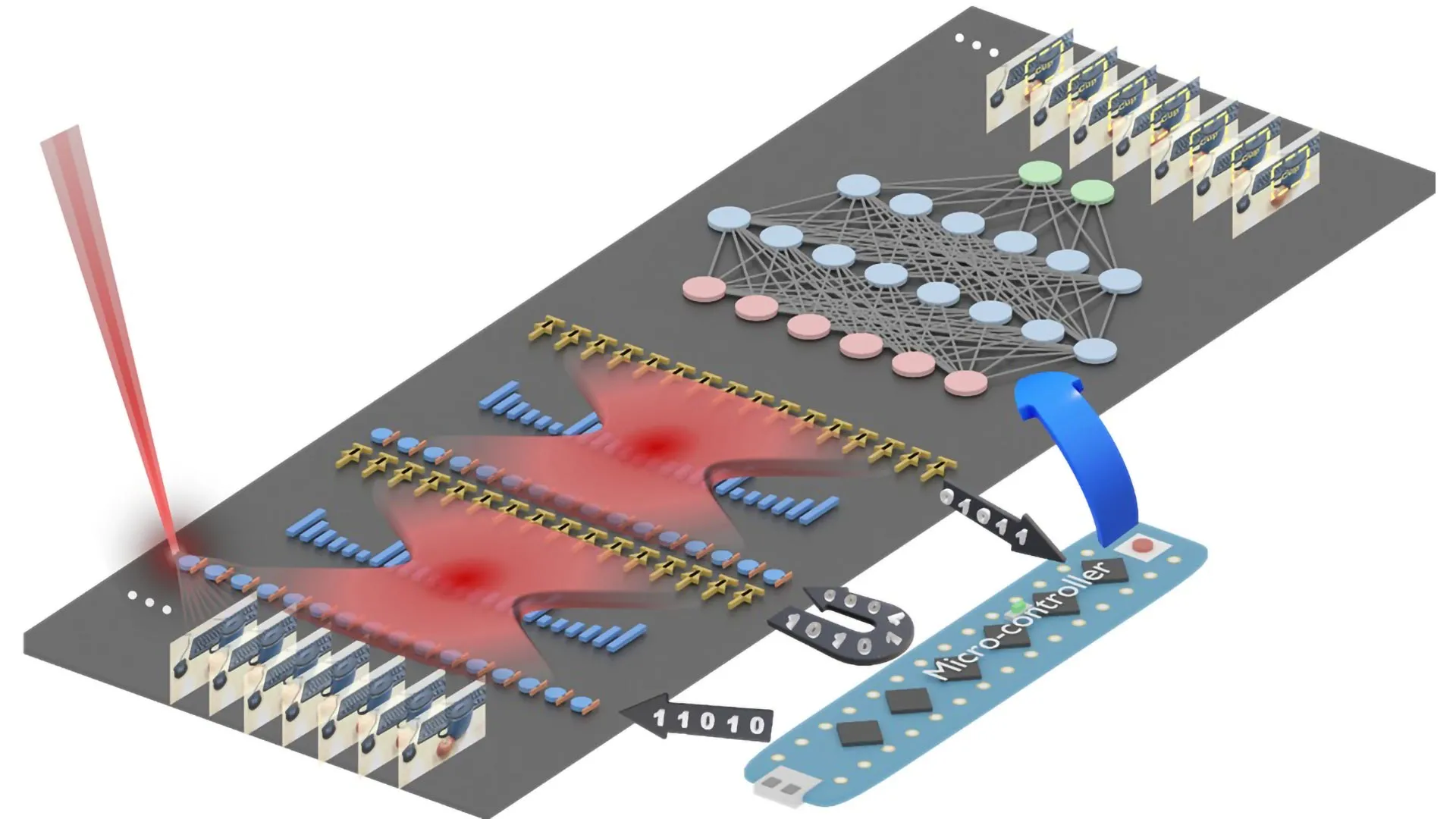
At the heart of this innovation lies the chip’s design to execute convolution operations, a fundamental computational process that forms the bedrock of machine learning. These operations are instrumental in enabling AI systems to discern intricate patterns within vast datasets, whether they are visual elements in images and videos or semantic structures in textual information. Traditionally, these convolutions demand substantial computing power, translating directly into high energy consumption. The University of Florida team has ingeniously overcome this hurdle by integrating optical components directly onto a silicon chip. This fusion of electronics and photonics allows the chip to perform convolutions using laser light and microscopic lenses, a paradigm shift that dramatically slashes energy consumption while simultaneously accelerating processing speeds.
The implications of this breakthrough are profound, as articulated by study leader Volker J. Sorger, the esteemed Rhines Endowed Professor in Semiconductor Photonics at the University of Florida. "Performing a key machine learning computation at near zero energy is a leap forward for future AI systems," Professor Sorger stated, underscoring the magnitude of their achievement. He further emphasized its critical importance for the continued expansion of AI capabilities in the years to come, "This is critical to keep scaling up AI capabilities in years to come." This advancement offers a tangible solution to the energy bottleneck that has threatened to stifle the exponential growth of AI.
The efficacy of this novel approach was rigorously tested and validated through prototype chip demonstrations. In benchmark tests, the chip successfully classified handwritten digits with an impressive accuracy of approximately 98 percent, a performance level directly comparable to that of conventional electronic chips. The technological marvel behind this efficiency lies in the chip’s architecture, which incorporates two sets of miniature Fresnel lenses. These lenses, a flat and ultrathin adaptation of the iconic lenses found in lighthouses, are fabricated using standard, scalable semiconductor manufacturing techniques. Measuring narrower than a human hair, these precisely etched lenses are seamlessly integrated directly onto the chip’s surface.
The operational mechanism of the chip for performing a convolution is elegantly simple yet remarkably effective. Machine learning data is first converted into laser light as it enters the chip. This light then traverses through the specially designed Fresnel lenses, which, through their unique optical properties, execute the necessary mathematical transformations required for the convolution. Following this optical computation, the resulting light signal is then reconverted into a digital signal, completing the AI task with unprecedented energy efficiency.
Hangbo Yang, a research associate professor in Professor Sorger’s group at UF and a co-author of the study, highlighted the novelty of their work: "This is the first time anyone has put this type of optical computation on a chip and applied it to an AI neural network." This statement emphasizes the pioneering nature of their research, which bridges the gap between optical physics and practical AI applications.
Furthermore, the research team showcased the chip’s remarkable capability to process multiple data streams concurrently. This feat is achieved by employing lasers emitting light of different colors, a sophisticated technique known as wavelength multiplexing. "We can have multiple wavelengths, or colors, of light passing through the lens at the same time," Professor Yang explained, elaborating on a key advantage of photonic integration. "That’s a key advantage of photonics." This ability to handle parallel processing streams through different wavelengths of light significantly amplifies the chip’s computational throughput and efficiency.
The collaborative spirit that fueled this innovation is also noteworthy. The research was a concerted effort involving multiple leading institutions, including the Florida Semiconductor Institute, the University of California, Los Angeles (UCLA), and George Washington University. Professor Sorger also pointed to the existing industry landscape, noting that established chip manufacturers like NVIDIA are already incorporating optical elements into certain aspects of their AI systems. This existing integration could significantly streamline the adoption and implementation of this new light-powered technology in future AI hardware.
Looking ahead, Professor Sorger expressed a clear vision for the future of AI hardware: "In the near future, chip-based optics will become a key part of every AI chip we use daily." He concluded with a bold prediction, "And optical AI computing is next," signifying the inevitable and transformative shift towards light-based computation for artificial intelligence. This research not only addresses the pressing need for energy efficiency in AI but also unlocks new avenues for computational performance and scalability, promising a future where artificial intelligence is both more powerful and more sustainable. The transition from purely electronic computation to optoelectronic and ultimately all-optical computing within AI chips represents a fundamental paradigm shift, akin to the transition from vacuum tubes to transistors, with the potential to redefine the limits of what AI can achieve. The implications extend beyond mere energy savings; they touch upon the very architecture of future computing, envisioning systems that are not only faster and more energy-efficient but also capable of tackling increasingly complex and data-intensive AI challenges that are currently beyond our reach. This light-powered chip is not just an incremental improvement; it is a beacon of innovation illuminating the path toward a more sustainable and advanced era of artificial intelligence.