Engineers have taken a major step toward producing the smallest earthquakes ever created, shrinking seismic-style vibrations down to the scale of a microchip, a breakthrough that promises to usher in an era of smaller, faster, and more energy-efficient wireless electronics, potentially miniaturizing your next smartphone and transforming the very fabric of modern communication.
The groundbreaking innovation centers on a novel device dubbed a surface acoustic wave (SAW) phonon laser. This cutting-edge technology, developed by a collaborative team from the University of Colorado Boulder, the University of Arizona, and Sandia National Laboratories, has the potential to unlock a new generation of advanced chips for smartphones, personal computers, and a vast array of other wireless devices. The research, meticulously detailed and published on January 14th in the prestigious journal Nature, marks a significant leap forward in harnessing and controlling mechanical vibrations at the nanoscale.
At the heart of this revolutionary technology lie surface acoustic waves, or SAWs. These ubiquitous phenomena, while often associated with the destructive power of large-scale earthquakes rippling across the Earth’s crust, also play a crucial, albeit less dramatic, role in our everyday lives. Unlike sound waves that propagate through a medium, SAWs are confined to the surface of a material, traveling along its outer layer. It is this precise, surface-bound nature that makes them invaluable in electronic applications.
"SAWs devices are critical to many of the world’s most important technologies," explained Matt Eichenfield, a senior author of the study and the incoming Gustafson Endowed Chair in Quantum Engineering at CU Boulder. His statement underscores the pervasive influence of SAWs, noting their presence in "all modern cell phones, key fobs, garage door openers, most GPS receivers, many radar systems and more." This highlights the fact that while the "phonon laser" itself is a new development, the underlying principle of using SAWs is already deeply embedded in the devices we rely on daily.
The current functionality of SAWs within smartphones provides a compelling illustration of their importance. Inside a typical mobile device, these minute mechanical vibrations act as highly sophisticated filters. When a radio signal arrives from a distant cell tower, it is first ingeniously converted into tiny mechanical oscillations. This transformation allows the phone’s internal chips to meticulously sift through the incoming signals, isolating the desired information from interference and background noise. Once the signal is cleaned and processed, these mechanical vibrations are then converted back into radio waves for transmission or reception.
The research team’s pivotal contribution lies in their development of a novel method for generating these surface waves, a process they have termed a "phonon laser." While a conventional laser emits beams of light, this newly engineered device produces controlled, coherent mechanical vibrations. "Think of it almost like the waves from an earthquake, only on the surface of a small chip," elaborated Alexander Wendt, a graduate student at the University of Arizona and the lead author of the study. This evocative analogy effectively conveys the scale and nature of the phenomenon being manipulated.
A key advantage of this new phonon laser design is its potential for integration and efficiency. Most existing SAW systems necessitate the use of two separate chips and an external power source. In stark contrast, the innovative design conceived by Eichenfield and his colleagues consolidates all necessary components onto a single chip. This consolidation not only promises a significant reduction in the physical footprint of electronic components but also opens the door for operation using a simple battery, all while achieving much higher operating frequencies than current SAW technologies.
To truly grasp the ingenuity of the phonon laser, it is beneficial to draw a parallel with the operation of conventional lasers. Many common lasers, such as those found in laser pointers and CD players, are diode lasers. These operate by bouncing light between two microscopic mirrors embedded within a semiconductor chip. As the light repeatedly reflects, it interacts with energized atoms within the semiconductor. These energized atoms, stimulated by the light, release additional photons, thereby amplifying the light beam.
Eichenfield elaborated on the significance of this analogy: "Diode lasers are the cornerstone of most optical technologies because they can be operated with just a battery or simple voltage source, rather than needing more light to create the laser like a lot of previous kinds of lasers. We wanted to make an analog of that kind of laser but for SAWs." This ambition to replicate the efficiency and practicality of diode lasers for mechanical vibrations underscores the transformative potential of their research.
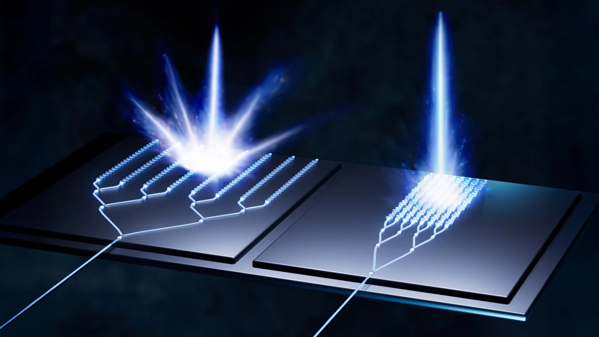
The physical realization of this phonon laser is a testament to precise engineering. The team constructed a bar-shaped device, approximately half a millimeter in length, which serves as the core of the vibration generation system. This compact structure is meticulously engineered from a stack of specialized materials, each playing a critical role in the device’s function.
At the foundation of this layered structure is silicon, the ubiquitous material that forms the backbone of virtually all modern computer chips. Resting atop the silicon is a thin layer of lithium niobate, a material renowned for its piezoelectric properties. Piezoelectric materials possess the remarkable ability to convert mechanical stress into electrical energy, and conversely, to generate mechanical vibrations when subjected to an electric field. This characteristic is crucial for initiating and sustaining the surface acoustic waves.
The uppermost layer is an exceptionally thin sheet of indium gallium arsenide. This material exhibits unusual electronic properties, allowing electrons to accelerate to extremely high speeds even under the influence of weak electric fields. The synergy between these layered materials is what enables the phonon laser to function. Specifically, the vibrations propagating along the surface of the lithium niobate layer can directly interact with the high-speed electrons within the indium gallium arsenide.
The researchers liken the operational principle of their device to that of a wave pool. When an electric current is applied to the indium gallium arsenide, it induces surface waves to form in the underlying lithium niobate layer. These waves then travel forward, strike a precisely engineered reflector, and bounce back. This continuous reflection, akin to light bouncing between mirrors in a traditional laser, is the mechanism by which the vibrations are amplified.
"It loses almost 99% of its power when it’s moving backward, so we designed it to get a substantial amount of gain moving forward to beat that," explained Wendt, highlighting the engineering challenge of overcoming wave dissipation. After undergoing numerous such forward and backward passes, the mechanical vibrations grow in amplitude, reaching a critical threshold where a portion of the amplified wave is emitted from one side of the device, analogous to how a laser beam exits its optical cavity.
The performance metrics achieved by this phonon laser are truly remarkable. The team successfully generated surface acoustic waves vibrating at a frequency of approximately 1 gigahertz, which translates to billions of oscillations per second. Crucially, the researchers are confident that the design can be further optimized to reach frequencies of tens or even hundreds of gigahertz. This represents a substantial improvement over traditional SAW devices, which typically have a frequency ceiling of around 4 gigahertz, making the new system significantly faster and more capable.
Eichenfield emphasized the far-reaching implications of this advance: "This advance could lead to wireless devices that are smaller, more powerful, and more energy efficient." The current architecture of smartphones, with their multiple chips dedicated to the repeated conversion of radio waves to SAWs and back again for every communication event, is a prime target for simplification. The ultimate goal of the researchers is to develop a single, integrated chip capable of handling all signal processing using surface acoustic waves, thereby streamlining device architecture and reducing power consumption.
"This phonon laser was the last domino standing that we needed to knock down," Eichenfield declared, signaling the culmination of years of dedicated research and development. "Now we can literally make every component that you need for a radio on one chip using the same kind of technology." This ambitious vision paints a picture of future wireless devices that are not only more compact and powerful but also more seamless and integrated, thanks to the groundbreaking capabilities of the phonon laser.