Published on February 23rd in the prestigious journal Nature Communications, the study was spearheaded by doctoral student Shake Karapetyan, with Professor David Muller of the Cornell Duffield College of Engineering leading the ambitious project. Muller, a distinguished figure in the field of materials science and engineering, highlighted the transformative potential of this new imaging technique, stating, "Since there’s really no other way you can see the atomic structure of these defects, this is going to be a really important characterization tool for debugging and fault-finding in computer chips, especially at the development stage." This sentiment underscores the critical need for such precise diagnostic capabilities as electronic components continue to shrink and become more intricate.
The semiconductor industry has historically grappled with the challenge posed by minuscule structural flaws. As the complexity of computer chips has escalated and their constituent elements have diminished to the scale of individual atoms, even the slightest irregularities can have a profound impact on device functionality. At the heart of every computer chip lies the transistor, a fundamental component that functions as an electronic switch, meticulously controlling the flow of electrical current. Within each transistor, a crucial channel opens and closes to govern the passage of electrons. Muller eloquently drew an analogy to illustrate this delicate balance: "The transistor is like a little pipe for electrons instead of water. You can imagine, if the walls of the pipe are very rough, it’s going to slow things down. And so measuring how rough the walls are and which walls are good and which walls are bad is now even more important." This analogy vividly captures how microscopic imperfections can impede the smooth operation of these critical components.
Professor Muller’s extensive career has been dedicated to exploring the physical limitations of semiconductor technology. His tenure at Bell Labs from 1997 to 2003 was instrumental in investigating the ultimate limits of transistor miniaturization. The evolution of transistor architecture on chips has been a fascinating journey. Initially, transistors were arranged in flat, planar layouts that spread across the chip’s surface, akin to urban sprawl. However, as engineers exhausted available surface area, they transitioned to a more efficient, three-dimensional stacking of transistors, creating intricate structures that resemble modern high-rise buildings. This vertical integration has allowed for an exponential increase in the number of transistors that can be packed onto a single chip.
The challenge, however, lies in the sheer scale of these modern 3D structures. Muller described them as being "smaller than the size of a virus. And these days, it’s a lot smaller. It’s more like a molecule-in-the-cell kind of scale." This diminishing size presents immense difficulties for diagnosis and repair. A single advanced chip today can house billions of transistors, and their shrinking dimensions make identifying and rectifying performance issues an increasingly formidable task. Karapetyan elaborated on this point, emphasizing the extreme precision required: "These days, a transistor channel can be only about 15 to 18 atoms wide, which is super, super tiny, and they’re extremely intricate. At this point, it matters where every atom is, and it’s really hard to characterize."
The breakthrough in visualizing these atomic-scale defects was made possible by significant advancements in electron microscopy. Earlier in his career at Bell Labs, Muller collaborated with Glen Wilk, now Vice President of Technology at ASM. Their joint research focused on finding alternatives to silicon dioxide, the prevalent gate material at the time, which suffered from excessive current leakage as devices became smaller. This pioneering work contributed to the widespread adoption of hafnium oxide, which subsequently became the standard material in computer processors and mobile devices from the mid-2000s onwards. Muller recalled the impact of their earlier research: "The papers we published on how to use electron microscopes to characterize these materials, I can tell you, a lot of the semiconductor folks had read those very, very carefully." He further likened the evolution of microscopy technology to a dramatic leap: "Back then, it was like flying biplanes. And now you’ve got jets."
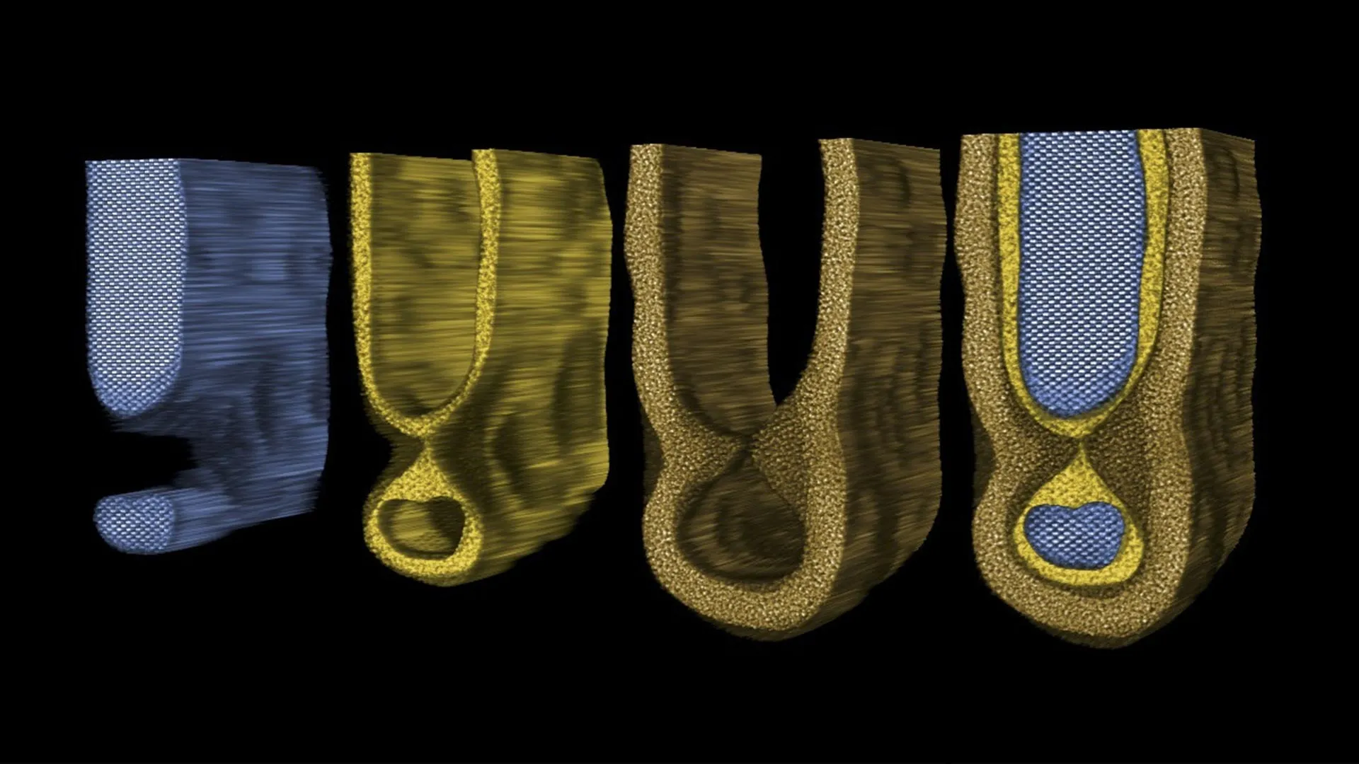
The "jet" Muller refers to is electron ptychography, a sophisticated computational imaging technique powered by an electron microscope pixel array detector (EMPAD). This detector, a co-development by Muller’s research group, meticulously records the intricate scattering patterns generated as electrons traverse the complex transistor structures. By precisely analyzing the shifts in these scattering patterns across different scan points, researchers can reconstruct remarkably detailed 3D images. The precision of this system is so extraordinary that it has achieved record-breaking resolution, enabling scientists to discern individual atoms with unparalleled clarity – a feat recognized by Guinness World Records.
The collaborative effort, reuniting Muller and Wilk after more than 25 years, alongside crucial support from TSMC and its Corporate Analytical Laboratories group, aimed to deploy the EMPAD technology to examine contemporary semiconductor devices. Karapetyan likened the process to "solving a massive puzzle, both in terms of taking the experimental data and doing the computational reconstruction." The rigorous analysis of the acquired and reconstructed imaging data allowed the researchers to pinpoint the exact positions of atoms within the transistor channels. This detailed mapping revealed subtle roughness at the interfaces of these channels, which Karapetyan aptly described as "mouse bites."
These "mouse bite" defects, it was discovered, originate during the highly optimized manufacturing processes employed for creating these advanced structures. The nanoelectronics research center Imec provided an ideal testbed for validating the imaging technique, offering sample devices that served as perfect canvases for observation. Karapetyan explained the intricate nature of modern chip fabrication: "Fabrication of modern devices takes hundreds, if not thousands, of steps of chemical etching and deposition and heating, and then every single step does something to your structure." The ability to now directly observe the results of each step, rather than relying on indirect projective imaging, offers a transformative advantage: "Before you used to look at projective images to try to figure out what was really going on. Now you have a direct probe to actually see after every single step and have a better grasp of, oh, I put the temperature this high, and then this is what it looks like." This granular insight into the fabrication process will undoubtedly lead to more robust and efficient manufacturing.
The implications of this newfound ability to directly observe atomic-level defects are profound and extend across a vast spectrum of electronic devices. From the ubiquitous smartphones and laptops that define our daily lives to the colossal data centers that form the backbone of the digital world, the performance of these technologies can now be scrutinized and improved with unprecedented precision. Furthermore, this advancement holds significant promise for the development of emerging technologies such as quantum computers, which demand an exceptionally high degree of control over material structures. Karapetyan expressed optimism for the future: "I think there’s a lot more science we can do now, and a lot more engineering control, having this tool."
The study’s co-authors include Steven Zeltmann, a staff scientist at the Platform for the Accelerated Realization, Analysis and Discovery of Interface Materials (PARADIM), and Ta-Kun Chen and Vincent Hou from TSMC. The research received crucial funding from TSMC, with support for the microscopy facilities provided by the Cornell Center for Materials Research (CCMR) and PARADIM, both of which are supported by the National Science Foundation. This multidisciplinary collaboration, fueled by significant financial and institutional backing, represents a monumental leap forward in our understanding and manipulation of the fundamental building blocks of modern technology.