Engineers have taken a monumental leap in miniaturizing seismic-style vibrations, shrinking them down to the scale of a microchip, a feat that could fundamentally reshape the future of our electronic devices. This groundbreaking advancement centers on a novel device dubbed a surface acoustic wave (SAW) phonon laser. The implications of this technology are far-reaching, holding the potential to enable the creation of vastly more advanced and efficient chips for smartphones and a wide array of other wireless electronics, ultimately leading to devices that are not only smaller but also significantly faster and more energy-efficient.
The pioneering research was spearheaded by Matt Eichenfield, an esteemed incoming faculty member at the University of Colorado Boulder, in collaboration with a talented team of scientists from the University of Arizona and Sandia National Laboratories. Their meticulously conducted findings, a culmination of extensive effort and innovation, were officially published on January 14th in the prestigious scientific journal, Nature.
Understanding the Power of Surface Acoustic Waves (SAWs)
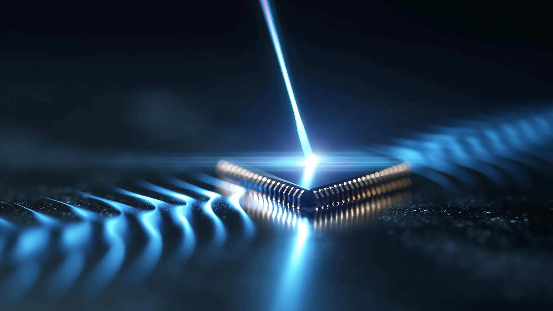
At the heart of this revolutionary new device lies the principle of surface acoustic waves, more commonly referred to by their acronym, SAWs. These fascinating waves share a conceptual kinship with sound waves, yet their behavior is distinct. Instead of propagating through the vast expanses of air or delving deep within the bulk of a material, SAWs are confined to travel exclusively along the very surface of a substance.
The dramatic power of these surface acoustic waves is perhaps most vividly illustrated by large-scale natural phenomena. Major earthquakes, for instance, unleash incredibly potent SAWs that radiate outwards across the Earth’s crust, causing widespread tremors that can shake buildings to their foundations and inflict considerable damage. However, on a far more subtle and controlled scale, SAWs have already become an indispensable component of our modern technological landscape.
"SAW devices are absolutely critical to the functioning of many of the world’s most important technologies," emphatically stated Eichenfield, who holds the distinguished position of senior author on this groundbreaking new study and serves as the Gustafson Endowed Chair in Quantum Engineering at CU Boulder. "You’ll find them integrated into every modern cell phone, they are essential in key fobs for unlocking cars, garage door openers, the vast majority of GPS receivers, and a significant number of radar systems, among many other applications."
The Integral Role of SAWs in Today’s Smartphones
Within the intricate circuitry of a typical smartphone, SAWs play a crucial role as exceptionally precise filters. When radio signals are received from a distant cell tower, they are initially transformed into minute mechanical vibrations. This conversion is a critical step that empowers the device’s chips to meticulously separate the desired, useful signals from the pervasive interference and background noise that are inherent in wireless communication. Once this crucial filtering process is complete, these cleaned and refined vibrations are then converted back into radio waves for further processing and transmission.
In this groundbreaking study, Eichenfield and his dedicated colleagues have introduced an entirely novel methodology for generating these vital surface waves. They have achieved this through the development of what they have termed a "phonon laser." In stark contrast to the familiar beam of light emitted by a typical laser pointer, this innovative device is engineered to produce precisely controlled mechanical vibrations.
"You can essentially think of it as analogous to the waves generated by an earthquake, but operating on the surface of a minuscule chip," explained Alexander Wendt, a diligent graduate student at the University of Arizona and the lead author of this pivotal study.
A significant limitation of most existing SAW systems is their reliance on multiple components. Typically, they require at least two separate chips and a dedicated external power source to function. The revolutionary new design developed by this team, however, ingeniously consolidates all necessary functionalities into a single, integrated chip. Furthermore, this advanced system possesses the remarkable capability to operate using only a standard battery while simultaneously achieving substantially higher operational frequencies than its predecessors.
Engineering a Laser Built for Vibrations
To truly appreciate the elegance and ingenuity of this new device, it is beneficial to first understand the fundamental principles behind how conventional lasers operate.
Many of the lasers we encounter in our daily lives are diode lasers. These remarkable devices generate light through a process of repeated reflection between two meticulously placed microscopic mirrors situated on a semiconductor chip. As the light bounces back and forth within this confined space, it interacts with atoms that have been energized by an electric current. These energized atoms, in turn, release additional photons, thereby amplifying and strengthening the light beam.
"Diode lasers have become the foundational cornerstone of a vast majority of optical technologies because they possess the significant advantage of being operable with a simple battery or a basic voltage source, rather than requiring an external light source to initiate laser operation, as was the case with many earlier types of lasers," Eichenfield elaborated. "Our core objective was to create a functional equivalent, an analog of that kind of laser, but specifically designed for SAWs."
To realize this ambitious goal, the research team meticulously engineered a bar-shaped device, measuring approximately half a millimeter in length – a size comparable to a grain of fine sand.
A Sophisticated Stack of Specialized Materials
The sophisticated construction of this phonon laser involves the precise layering of several distinct and specialized materials. At its foundational base lies silicon, the ubiquitous and fundamental material that forms the backbone of most modern computer chips. Positioned directly above the silicon substrate is a remarkably thin layer of lithium niobate, a material renowned for its piezoelectric properties. Piezoelectric materials possess the unique characteristic of generating oscillating electric fields when subjected to mechanical vibrations, and conversely, these electric fields can also induce mechanical vibrations.
Crowning this layered structure is an exceptionally thin sheet of indium gallium arsenide. This material exhibits unusual and highly advantageous electronic properties, most notably its ability to accelerate electrons to extremely high speeds, even when exposed to relatively weak electric fields.
When these meticulously selected layers are assembled and activated, they facilitate a direct and powerful interaction between the surface acoustic waves propagating along the lithium niobate surface and the high-speed electrons residing within the indium gallium arsenide layer. This synergistic interplay is the key to the device’s ability to amplify and sustain the surface waves.
Constructing Waves That Build Like a Laser
The researchers adeptly describe the operational mechanism of their phonon laser using an analogy to a wave pool.
When an electric current is introduced and flows through the indium gallium arsenide layer, it initiates the formation of surface waves within the underlying lithium niobate layer. These waves then begin to travel forward, encounter a meticulously placed reflector, and subsequently rebound, traveling backward. This process is remarkably similar to how light reflects between the mirrors within a conventional laser cavity. With each forward pass, the wave gains energy and strength, while each backward pass, due to inherent inefficiencies, results in a loss of power.
"It loses almost 99% of its power when it’s moving backward, so we strategically designed the system to achieve a substantial amount of energy gain during its forward propagation, ensuring it could overcome these losses," explained Wendt.
After undergoing numerous such passes and reflections, the surface vibrations progressively grow in amplitude and intensity. Eventually, they become sufficiently strong that a portion of this amplified wave energy is permitted to escape from one side of the device, mirroring the way a laser beam eventually exits its optical cavity.
Achieving Faster Waves and Even Smaller Devices
Leveraging this innovative approach, the research team successfully generated surface acoustic waves that vibrated at an impressive frequency of approximately 1 gigahertz, signifying billions of oscillations occurring every single second. Moreover, the researchers are highly optimistic that the inherent design principles of this phonon laser could be further optimized and pushed to achieve even higher frequencies, potentially reaching tens or even hundreds of gigahertz.
In stark contrast, traditional SAW devices typically operate at their maximum capacity around 4 gigahertz. This makes the newly developed system a significant advancement, offering speeds that are orders of magnitude faster.
Eichenfield highlighted the profound impact this technological leap could have on the development of wireless devices. He envisions a future where these devices will be noticeably smaller, possess considerably greater processing power, and consume significantly less energy, leading to longer battery life and a more sustainable electronic ecosystem.
He further elaborated on the current inefficiencies in modern smartphones, where numerous chips are repeatedly engaged in the complex process of converting radio waves into SAWs and then back again, a cycle that occurs every time a user sends a message, makes a call, or browses the internet. The ultimate ambition of the researchers is to drastically simplify this convoluted process by creating a single, unified chip capable of handling all essential signal processing functions exclusively through the manipulation of surface acoustic waves.
"This phonon laser represented the final, critical barrier that we needed to overcome," Eichenfield concluded, his voice filled with a sense of accomplishment. "Now, we possess the capability to literally fabricate every single component required for a radio transceiver on a single chip, all utilizing the same foundational technological principles."