Unlike the predominantly flat, two-dimensional (2D) chips that characterize most of today’s computing infrastructure, this pioneering prototype is engineered with a vertical orientation. Its design is akin to a towering skyscraper, where ultra-thin components are stacked like successive floors. This vertical stacking is complemented by an intricate network of vertical wiring, functioning as an array of high-speed elevators capable of transporting immense volumes of data with unprecedented rapidity. The chip boasts a record-breaking number of vertical interconnections and an exceptionally dense, interwoven layout that strategically positions memory and computing units in close proximity. This integrated design effectively circumvents the data transfer slowdowns that have historically constrained the performance of conventional flat chips. In rigorous hardware tests and sophisticated simulations, this new 3D chip has demonstrated a performance advantage of approximately an order of magnitude over its 2D counterparts.
While experimental 3D chips have been conceived and built in academic laboratories previously, this development marks a significant milestone as the first time such a chip has delivered demonstrable performance improvements and, crucially, has been manufactured in a commercial foundry. "This opens the door to a new era of chip production and innovation," declared Subhasish Mitra, the William E. Ayer Professor in Electrical Engineering and professor of computer science at Stanford University, and the principal investigator of a new paper detailing the chip, which was presented at the 71st Annual IEEE International Electron Devices Meeting (IEDM). He further emphasized, "Breakthroughs like this are how we get to the 1,000-fold hardware performance improvements future AI systems will demand."
The Inherent Limitations of Flat Chips in Modern AI Architectures
The immense scale of contemporary AI models, such as those powering platforms like ChatGPT and Claude, necessitates the constant and rapid movement of vast quantities of data between memory units, which store information, and the processing cores that execute computations. On conventional 2D chips, where all components reside on a single plane, memory is often limited in capacity and distributed across the chip. This spatial separation forces data to traverse lengthy and congested pathways, creating a significant bottleneck. The processing units within these chips are capable of operating at speeds far exceeding the rate at which data can be supplied from memory, and the chip struggles to maintain sufficient memory close to the processing elements. The consequence is pervasive waiting periods, a phenomenon engineers refer to as the "memory wall," where the processing capabilities are hampered by the chip’s inability to efficiently feed it data.
For an extended period, chip manufacturers have attempted to push back against this memory wall by relentlessly shrinking transistors – the fundamental building blocks of integrated circuits responsible for computation and data storage – and by increasing their density on each chip. However, researchers now assert that this approach is rapidly approaching its hard physical limitations, often termed the "miniaturization wall."
The innovative design of this new 3D chip is strategically engineered to surmount both these formidable barriers by embracing verticality. "By integrating memory and computation vertically, we can move a lot more information much quicker, just as the elevator banks in a high-rise let many residents travel between floors at once," explained Tathagata Srimani, assistant professor of electrical and computer engineering at Carnegie Mellon University and the paper’s senior author. Srimani, who initiated this research as a postdoctoral fellow under Mitra’s guidance, highlighted the analogy of efficient vertical transport for data.
Robert M. Radway, assistant professor of electrical and systems engineering at the University of Pennsylvania and a co-author of the study, articulated the severity of the challenge: "The memory wall and the miniaturization wall form a deadly combination." He continued, "We attacked it head-on by tightly integrating memory and logic and then building upward at extremely high density. It’s like the Manhattan of computing — we can fit more people in less space." This metaphor vividly illustrates the dense, efficient utilization of space achieved by the 3D architecture.
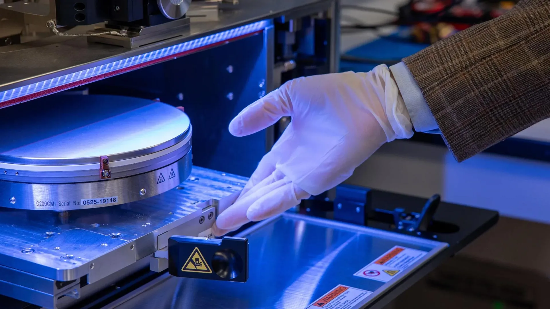
The Manufacturing Process of the Monolithic 3D Chip
Previous endeavors in developing 3D chips have often adopted a more straightforward approach, involving the stacking of pre-manufactured, separate chips. While this method can offer some advantages, the interconnections between these stacked layers are typically less robust, limited in number, and can themselves become performance bottlenecks.
The research team behind this new chip has adopted a fundamentally different and more sophisticated methodology. Instead of fabricating individual chips and then bonding them together, they construct each successive layer directly atop the preceding one in a seamless, continuous manufacturing flow. This advanced technique, known as "monolithic" 3D integration, employs processing temperatures that are sufficiently low to prevent damage to the circuitry already established in the lower layers. This critical capability enables the layers to be stacked with much greater intimacy and facilitates the creation of a significantly denser network of connections between them.
A particularly noteworthy aspect of this achievement, as emphasized by the researchers, is that the entire manufacturing process was successfully executed within a domestic commercial silicon foundry. "Turning a cutting-edge academic concept into something a commercial fab can build is an enormous challenge," stated Mark Nelson, vice president of technology development operations at SkyWater Technology and a co-author of the paper. He underscored the broader implications: "This shows that these advanced architectures aren’t just possible in the lab — they can be produced domestically, at scale, which is what America needs to stay at the forefront of semiconductor innovation." This collaboration signifies a critical step in translating theoretical breakthroughs into tangible, scalable manufacturing capabilities within the United States.
Performance Gains and the Future Trajectory of AI Hardware
Initial hardware tests of the prototype have yielded impressive results, with the 3D chip outperforming comparable 2D chips by approximately fourfold. Furthermore, the team’s extensive simulations suggest that the performance gains will become even more substantial as the design is scaled up, incorporating additional stacked layers of memory and compute. Projections indicate that with further vertical expansion, the models could achieve up to a twelvefold improvement in performance on realistic AI workloads, including those derived from Meta’s open-source LLaMA model.
Beyond immediate performance enhancements, the researchers highlight a significant long-term benefit. They posit that this architecture offers a practical pathway to achieving improvements of 100 to 1,000 fold in the Energy Delay Product (EDP). EDP is a crucial metric that quantifies the combined efficiency of a chip in terms of both its speed and its energy consumption. By drastically reducing the distances data must travel and by introducing a multitude of parallel vertical pathways for data movement, the chip can simultaneously boost throughput and decrease the energy required per operation – a combination that has proven exceptionally challenging to attain with traditional flat chip designs.
The significance of this research extends beyond mere performance metrics. By demonstrating the feasibility of manufacturing monolithic 3D chips within the United States, the team asserts that this work provides a foundational blueprint for a new era of domestic hardware innovation. This new era envisions the design and fabrication of the most advanced chips on U.S. soil, fostering technological sovereignty and economic competitiveness.
Moreover, the transition to vertical, monolithic 3D integration will necessitate the cultivation of a new generation of engineers proficient in these advanced methodologies. This is analogous to the transformative impact of the integrated circuit boom in the 1980s, which was significantly propelled by students acquiring expertise in chip design and fabrication within U.S. laboratories. Through robust collaborations and dedicated funding initiatives, such as those supported by the Microelectronics Commons California-Pacific-Northwest AI Hardware Hub (Northwest-AI-Hub), students and researchers are actively being prepared to drive American semiconductor innovation forward.
"Breakthroughs like this are of course about performance," affirmed H.-S. Philip Wong, the Willard R. and Inez Kerr Bell Professor in the Stanford School of Engineering and a principal investigator of the Northwest-AI-Hub. "But they’re also about capability. If we can build advanced 3D chips, we can innovate faster, respond faster, and shape the future of AI hardware." This sentiment encapsulates the dual promise of enhanced performance and expanded technological capability that this new 3D chip architecture represents.
The research was conducted across prestigious institutions including the Stanford University School of Engineering, Carnegie Mellon University College of Engineering, the University of Pennsylvania School of Engineering and Applied Science, and the Massachusetts Institute of Technology. All fabrication processes were executed at SkyWater Technology’s facility in Bloomington, Minnesota. The project received substantial support from a diverse range of entities, including the Defense Advanced Research Projects Agency, the U.S. National Science Foundation Graduate Research Fellowship Program, Samsung, the Stanford Precourt Institute for Energy, the Stanford SystemX Alliance, the Department of War’s Microelectronics Commons AI Hardware Hub, the U.S. Department of Energy, and the National Science Foundation’s Future of Semiconductors Program (grant number 2425218).
Additional Stanford co-authors contributing to this seminal work include Suhyeong Choi, Samuel Dayo, Andrew Bechdolt, Shengman Li, Dennis T. Rich, and R.H. Yang. Further contributions were made by researchers from Carnegie Mellon University and the Massachusetts Institute of Technology, underscoring the truly collaborative and interdisciplinary nature of this significant technological leap.