

 Imroatul Nasiyah
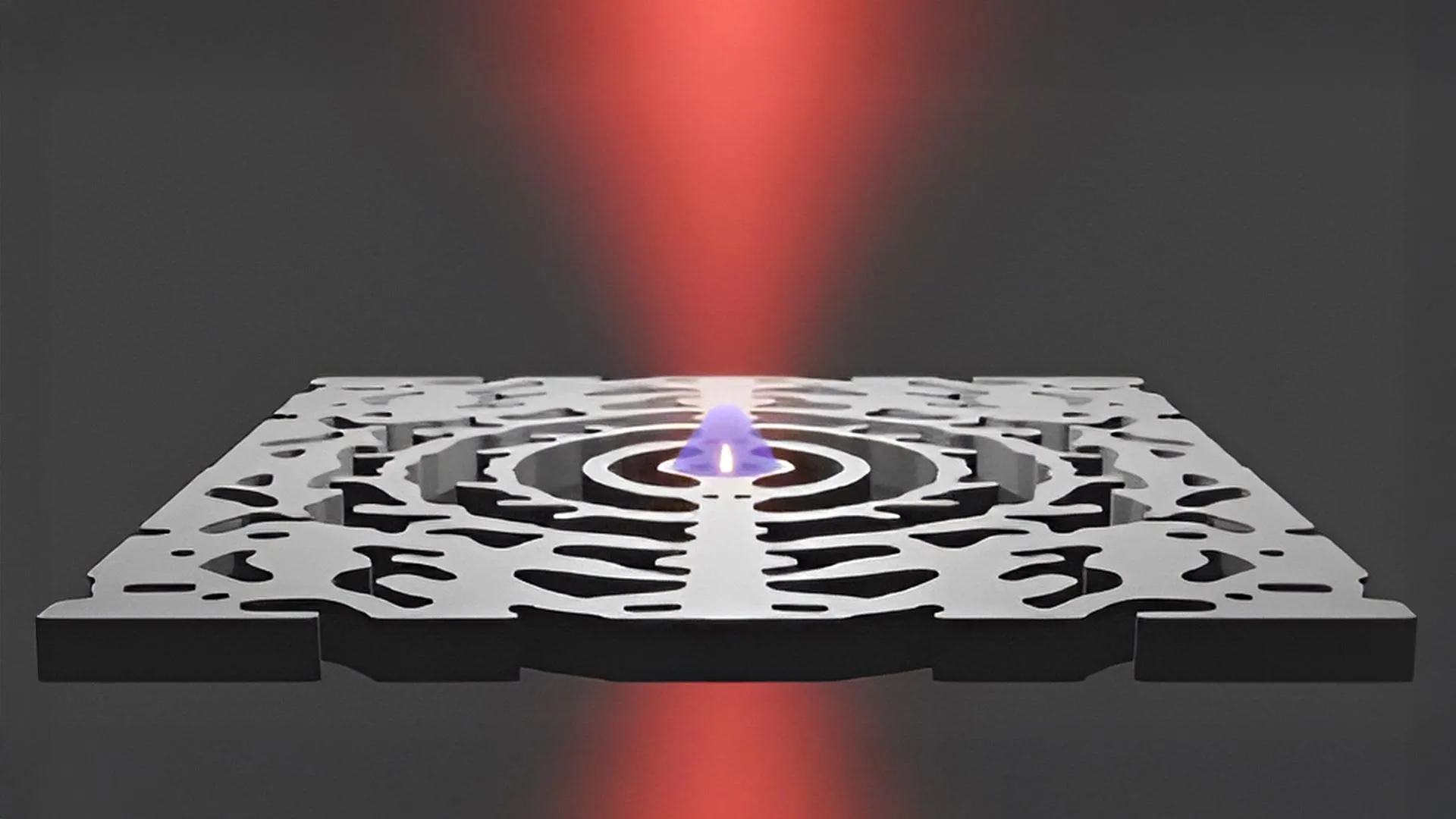
The development of a revolutionary nanolaser by researchers at the Technical University of Denmark (DTU) heralds a significant leap towards a future where microchips communicate entirely through particles of light, promising to slash computer energy consumption by up to 50%. This breakthrough, detailed in the prestigious scientific journal Science Advances, could fundamentally reshape the landscape of computing, smartphones, and vast data centers, making them not only faster but also dramatically more energy-efficient.
For decades, the intricate dance of information within our digital devices has been orchestrated by electrical signals coursing through circuits. While this method has powered the digital revolution, it comes with inherent limitations. Electrical signals generate heat, a ubiquitous byproduct that not only necessitates complex cooling systems but also acts as a bottleneck, restricting the speed at which data can be processed and transmitted. This is where the elegant simplicity of light, in the form of photons, offers a compelling alternative. Much of the internet’s backbone already relies on the speed and efficiency of light traveling through fiber optic cables. Now, the ambition is to bring this optical communication paradigm directly onto the microchip itself.
The DTU nanolaser represents a pivotal early step in this ambitious endeavor. Imagine a future where thousands, perhaps even millions, of these minuscule lasers are integrated onto a single microchip. Instead of electrons carrying data across the silicon, it would be photons. This shift from electrical to optical communication within a chip promises to overcome the limitations of heat generation and speed, enabling devices to operate with significantly less energy loss. Professor Jesper Mørk, a leading figure in this research at DTU, elaborates on the profound implications: "The nanolaser opens up the possibility of creating a new generation of components that combine high performance with minimal size. This could be in information technology, for example, where ultra-small and energy-efficient lasers can reduce energy consumption in computers, or in the development of sensors for the healthcare sector, where the nanolaser’s extreme light concentration can deliver high-resolution images and ultrasensitive biosensors."
The core of this innovative nanolaser lies in its ability to break through conventional size limitations for laser technology. Crafted within the pristine environment of DTU’s clean room facility, DTU Nanolab, this device utilizes a sophisticated structure known as a nanocavity. This nanocavity acts as an exceptionally tiny trap, concentrating light within an incredibly small volume. Achieving such intense light confinement at this minuscule scale was previously considered an immense technological hurdle. The magic happens when researchers direct a beam of light onto the device. This interaction causes both photons and electrons to converge in the same microscopic region. This synergy allows the laser to function efficiently at room temperature, a crucial factor for practical applications, and demands remarkably little energy to operate. The underlying light-trapping structure itself is a testament to collaborative innovation, having been originally developed by Professor Ole Sigmund’s group at DTU Construct.
The potential impact of this technology on energy consumption is staggering. Professor Mørk estimates that the widespread adoption of nanolasers in computers could lead to a reduction in energy usage by as much as half. This is not a trivial improvement; in a world increasingly reliant on digital infrastructure, such an efficiency gain could translate into monumental energy savings and a significant reduction in the carbon footprint of computing. Data centers, notorious for their voracious energy appetite, stand to benefit immensely. Imagine these power-hungry facilities operating with half the electricity consumption, a change that would have far-reaching environmental and economic consequences.
Beyond computing, the implications for healthcare are equally transformative. The nanolaser’s unparalleled ability to concentrate light into an extremely confined space opens doors for the development of ultra-sensitive sensors. These sensors could revolutionize disease detection, enabling earlier and more accurate diagnoses. Furthermore, the technology holds promise for high-resolution imaging systems, potentially offering unprecedented detail in medical scans and diagnostics.
While the current nanolaser operates by being stimulated by external light, the next critical hurdle for researchers is to enable it to function using electrical power. Achieving this milestone would unlock the full potential of this technology, paving the way for its seamless integration into the components we use every day. The team at DTU is optimistic, estimating that the remaining technical challenges could be overcome within the next 5 to 10 years. This timeline suggests that the era of light-speed communication within our devices, and the consequent energy revolution it promises, is not a distant dream but a tangible near-future reality.
The journey from a laboratory breakthrough to widespread commercial adoption is often long and complex, but the DTU nanolaser represents a profound and encouraging stride forward. It exemplifies the power of interdisciplinary research, combining expertise in optics, materials science, and nanotechnology to address some of the most pressing challenges in modern technology. As we continue to push the boundaries of what is possible with microelectronics, the humble nanolaser, born from the pursuit of fundamental scientific understanding, may well become the unsung hero that powers a more efficient, faster, and sustainable digital future. The ability to move beyond the limitations of electrons and embrace the inherent speed and efficiency of photons within our chips is no longer science fiction; it is a developing scientific and engineering reality.