The world’s most advanced data centers are on the cusp of a radical transformation, with the ancient material of glass poised to become the foundation for next-generation artificial intelligence chips. South Korean company Absolics is spearheading this revolution, with plans to commence commercial production of specialized glass panels this year, designed to significantly enhance the power and energy efficiency of high-performance computing hardware. This burgeoning trend is not an isolated endeavor; industry giants like Intel are also investing heavily in this area, signaling a potential paradigm shift that could dramatically reduce the energy demands of AI data centers and, eventually, trickle down to consumer electronics such as laptops and mobile devices as production costs decrease.
The core innovation lies in utilizing glass as a substrate, the foundational layer upon which multiple silicon chips are interconnected. This sophisticated "packaging" technique is increasingly favored in modern computing hardware development, as it enables engineers to seamlessly integrate specialized chips, each optimized for distinct functions, into a unified system. However, this approach presents significant engineering challenges, particularly concerning thermal management. The immense heat generated by high-performance chips can cause conventional substrates to warp, leading to misaligned components, compromised cooling efficiency, and a heightened risk of damage or premature failure. Deepak Kulkarni, a senior fellow at chip design firm Advanced Micro Devices (AMD), highlights this critical issue, stating, "As AI workloads surge and package sizes expand, the industry is confronting very real mechanical constraints that impact the trajectory of high-performance computing. One of the most fundamental is warpage."
Glass emerges as a compelling solution to this escalating problem. Its superior thermal stability allows it to withstand the intense heat generated by AI processors far better than current organic substrates. This resilience enables engineers to further miniaturize chip packages, leading to enhanced speed and energy efficiency. Kulkarni elaborates on this advantage, noting that glass "unlocks the ability to keep scaling package footprints without hitting a mechanical wall."
The momentum behind this transition is palpable. Absolics has already established a dedicated factory in the United States for producing glass substrates for advanced chips and anticipates launching commercial manufacturing imminently. Intel, a titan in semiconductor manufacturing, is actively working to integrate glass into its next-generation chip packages, and its research efforts are galvanizing investment across the chip packaging supply chain. Early adopters are emerging from both South Korea and China. Bilal Hachemi, a senior technology and market analyst at Yole Group, observes, "Historically, this is not the first attempt to adopt glass in semiconductor packaging. But this time, the ecosystem is more solid and wider; the need for glass-based [technology] is sharper."
For decades, chip packaging has relied on organic substrates, such as fiberglass-reinforced epoxy, since the 1990s. However, these materials present inherent limitations. Rahul Manepalli, vice president of advanced packaging at Intel, explains that electrochemical complications restrict the proximity of drilled holes used for creating copper-coated signal and power connections between chips and the broader system. Furthermore, designers must contend with the unpredictable shrinkage and distortion that organic substrates undergo as chips cycle through heating and cooling phases. Manepalli recalls a realization within Intel about a decade ago: "We realized about a decade ago that we are going to have some limitations with organic substrates."

Glass, with its distinct properties, promises to overcome many of these limitations. Its remarkable thermal stability could facilitate the creation of up to ten times more connections per millimeter compared to organic substrates, according to Manepalli. This increased connectivity allows Intel’s designers to incorporate 50% more silicon chips within the same package area, significantly boosting computational power. The denser connections also optimize the routing of copper wires that supply power to the chips. Crucially, glass’s superior heat dissipation capabilities enable the design of more energy-efficient chips, thereby reducing overall power consumption. Manepalli emphatically states, "The benefits of glass core substrates are undeniable. It’s clear that the benefits will drive the industry to make this happen sooner rather than later, and we want to be one of the first ones who do it."
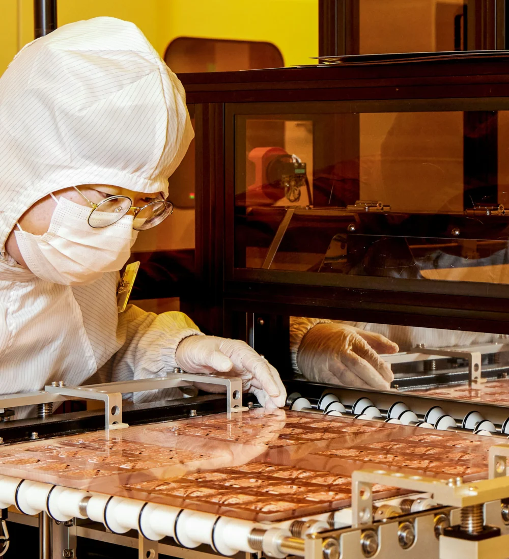
Despite its promising attributes, working with glass introduces its own set of challenges. Its inherent fragility is a primary concern. Manepalli notes that glass substrates for data center chip packages are manufactured from panels measuring only about 700 micrometers to 1.4 millimeters thick, rendering them susceptible to cracking or shattering. For years, researchers at Intel and other institutions have dedicated considerable effort to developing techniques and specialized tools to safely integrate these delicate glass panels into semiconductor manufacturing processes.
However, significant progress has been made. Manepalli reports that Intel’s research and development teams are now reliably fabricating glass panels and producing test chip packages that incorporate them. In early 2025, they successfully demonstrated a functional device with a glass core substrate booting up the Windows operating system, a remarkable achievement compared to the early testing phases where hundreds of glass panels would fracture every couple of days.
While semiconductor manufacturers already employ glass for more constrained applications, such as temporary support structures for silicon wafers, the potential market for glass substrates is substantial. Independent market research firm IDTechEx projects that the semiconductor market for glass could expand from $1 billion in 2025 to as much as $4.4 billion by 2036.
The potential benefits of glass extend beyond its mechanical and thermal properties. Glass can be manufactured to an astonishing degree of smoothness – 5,000 times smoother than organic substrates. Xiaoxi He, a research analyst at IDTechEx, explains that this ultra-smooth surface minimizes defects that can arise during the layering of metal onto semiconductors, which can degrade chip performance or render them inoperable.
Furthermore, glass holds the key to accelerating data transfer speeds. Its ability to guide light opens avenues for chip designers to embed high-speed signal pathways directly within the substrate. Kulkarni at AMD envisions this as a pivotal advancement for energy-efficient AI computation, stating, "Glass holds enormous potential for the future of energy-efficient AI compute." This light-based system could transmit signals with significantly less energy than the "power-hungry" copper pathways currently used for inter-chip communication.

The journey of glass packaging research began in 2009 at the 3D Systems Packaging Research Center at the Georgia Institute of Technology. This academic endeavor eventually led to a partnership with Absolics, a subsidiary of SKC, a South Korean company renowned for its expertise in chemicals and advanced materials. SKC established a semiconductor facility in Covington, Georgia, in 2024, specifically for manufacturing glass substrates. The collaborative efforts between Absolics and Georgia Tech were further bolstered by two grants totaling $175 million in the same year, awarded through the U.S. government’s CHIPS for America program.
Absolics is now transitioning to commercialization, with plans to begin producing small quantities of glass substrates for customers this year. Yongwon Lee, a research engineer at Georgia Tech not directly involved in the commercial partnership, acknowledges Absolics’ pioneering role in bringing glass substrates to market. Absolics’ current facility has an annual production capacity of 12,000 square meters of glass panels, which Lee estimates is sufficient to supply glass substrates for approximately 2 million to 3 million chip packages of the scale of Nvidia’s H100 GPU.
However, Absolics is not operating in isolation. Lee notes that several major manufacturers, including Samsung Electronics, Samsung Electro-Mechanics, and LG Innotek, have "significantly accelerated" their research and pilot production efforts in glass packaging over the past year. This collective surge in activity indicates that the glass substrate ecosystem is evolving from a single early innovator to a broader, more competitive industrial race.
Other companies are strategically positioning themselves within the specialized roles of the glass substrate supply chain. In 2025, JNTC, a company specializing in electrical connectors and tempered glass for electronics, inaugurated a facility in South Korea capable of producing 10,000 semi-finished glass panels per month. These panels feature pre-drilled holes for vertical electrical connections and thin metal layers, but they require further manufacturing processes for integration into chip packages. JNTC began accepting orders for these semi-finished glass components from specialized substrate companies and semiconductor manufacturers last year. The company plans to expand its production capacity in 2026 and establish an additional manufacturing line in Vietnam by 2027. These industry-wide developments underscore the rapid transition of glass substrate technology from prototype to commercial viability and highlight the widespread conviction among tech players that glass represents a surprisingly robust foundation for the future of computing and artificial intelligence.