

 Imroatul Nasiyah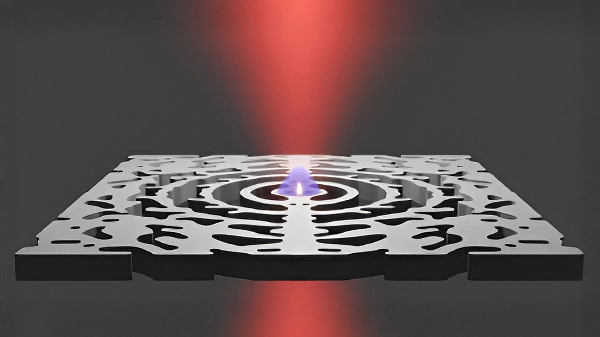
The core innovation lies in the ability to integrate thousands of these minuscule lasers onto a single microchip. This opens the door to a paradigm shift in how data is processed and transmitted within electronic devices. Currently, information travels across microchips via electrical signals, a method that generates heat and imposes inherent limitations on speed. The DTU nanolaser offers a compelling alternative: utilizing photons, the fundamental particles of light, to carry data. This "optical computing" approach promises to circumvent the limitations of electrical signaling, leading to faster, cooler, and significantly more energy-efficient devices.
Professor Jesper Mørk, a leading figure in the research and co-author of the study, emphasizes the transformative potential of this nanolaser. "The nanolaser opens up the possibility of creating a new generation of components that combine high performance with minimal size," he stated. "This could be in information technology, for example, where ultra-small and energy-efficient lasers can reduce energy consumption in computers, or in the development of sensors for the healthcare sector, where the nanolaser’s extreme light concentration can deliver high-resolution images and ultrasensitive biosensors." The research team, which also includes Drs. Meng Xiong and Yi Yu from DTU Electro, has successfully demonstrated a device that pushes the boundaries of miniaturization for laser technology.
The concept of using light for data transmission is already a cornerstone of modern communication networks. The internet, for instance, relies heavily on fiber optic cables to ferry vast amounts of information using light signals. However, the internal workings of computers have largely remained tethered to electrical circuits. This reliance on electricity to move data within chips is a major contributor to energy waste and heat generation. Electrical signals encounter resistance as they travel, leading to energy loss and the need for complex cooling systems. Nanolasers have the potential to bridge this gap, bringing the efficiency of optical communication directly onto the microchip. By generating light signals within the chip itself, these lasers can facilitate data transfer with minimal energy dissipation, paving the way for devices that are not only faster but also significantly more energy-efficient.
Professor Mørk projects that the integration of nanolasers into computers could lead to an astonishing reduction in energy consumption, potentially cutting it in half. This is a staggering figure when considering the immense power demands of today’s digital infrastructure, from personal laptops to sprawling data centers. The compact nature of the DTU nanolaser is a crucial step towards this ambitious goal. Future chips designed for optical communication will likely require a dense array of thousands of these highly efficient lasers, working in concert to transmit data across the intricate pathways of the microchip.
The achievement of creating such a tiny laser represents a significant leap in overcoming the fundamental physical constraints that have historically limited laser size. The heart of the DTU nanolaser lies in a novel structure known as a nanocavity. This carefully engineered element is designed to trap and concentrate light within an extraordinarily small volume. Previously, achieving such intense light confinement at the nanoscale was considered an exceptionally difficult engineering challenge. The researchers have managed to overcome this hurdle by creating a design that precisely manipulates light at the atomic level.
The groundbreaking mechanism of the nanolaser involves the simultaneous concentration of both photons and electrons within the same microscopic region. When a beam of light is directed at the device, it interacts with electrons in a way that triggers the emission of more light, creating a self-sustaining laser effect. This interaction is so efficient that the nanolaser can operate effectively at room temperature, a significant advantage over many existing laser technologies that require cryogenic cooling. Furthermore, this process demands an unusually low amount of energy to initiate and sustain the laser beam. The sophisticated light-trapping structure employed in this nanolaser was itself a product of prior innovation, originally developed by Professor Ole Sigmund’s group at DTU Construct, highlighting a collaborative spirit within the university.
The next critical hurdle for the widespread adoption of this technology is to enable the nanolaser to operate using electrical power. Currently, an external light source is used to activate the laser. If researchers can successfully develop an electrical pumping mechanism, the nanolaser’s applications will broaden exponentially across computing, telecommunications, and healthcare. The implications for the computing industry are profound. Personal computers and smartphones could experience unprecedented performance boosts while consuming a fraction of the electricity they do today. This would not only benefit individual users through longer battery life and reduced heat but also contribute to a more sustainable technological ecosystem.
Data centers, which are notorious for their gargantuan power appetites, stand to benefit immensely. A significant reduction in their energy consumption could translate into substantial cost savings and, more importantly, a considerable decrease in their environmental footprint. The potential climate benefits of widespread adoption of this technology are therefore immense. Beyond the realm of information technology, the nanolaser’s ability to concentrate light into an infinitesimally small area holds immense promise for advancements in healthcare. It could form the basis for ultra-sensitive biosensors capable of detecting diseases at their earliest stages with unparalleled accuracy. Furthermore, its precise light control could lead to the development of high-resolution imaging systems, enabling medical professionals to visualize biological structures with remarkable clarity, potentially revolutionizing diagnostics and treatment planning.
The researchers are optimistic about the timeline for overcoming the remaining technical challenges. They estimate that the necessary advancements to bring the nanolaser to full commercial viability could be achieved within the next five to ten years. This relatively short timeframe underscores the rapid pace of innovation in the field of photonics and the significant potential of this tiny, yet powerful, device to shape the future of technology. The development of this nanolaser is not merely an incremental improvement; it represents a fundamental shift in how we can conceive of and build the electronic devices that power our modern world, promising a future that is both more capable and significantly more sustainable.