
 Imroatul Nasiyah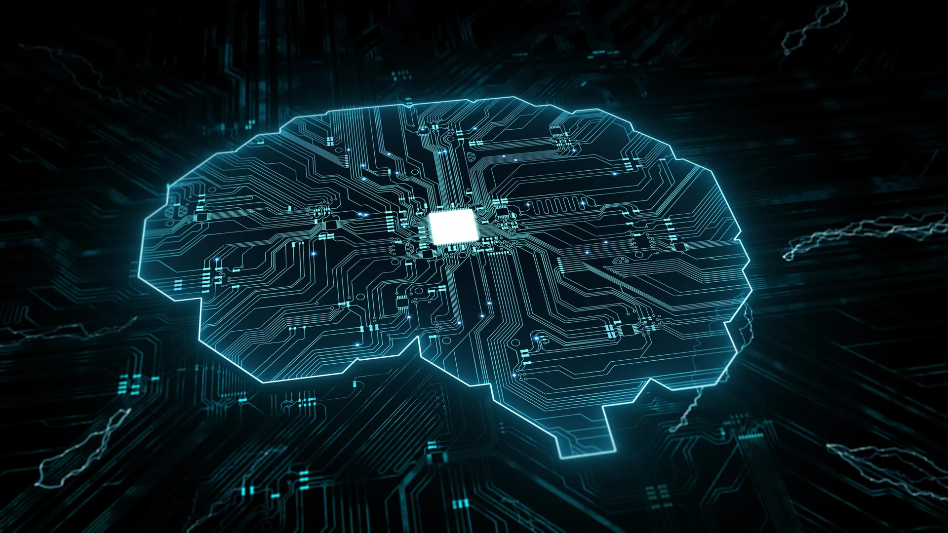
The core of this innovation lies in a novel method for generating and precisely controlling negative differential resistance (NDR) within industry-standard Silicon Carbide (SiC) Metal-Oxide-Semiconductor Field-Effect Transistors (MOSFETs). NDR is a peculiar electronic phenomenon where an increase in voltage across a device leads to a decrease in current, a characteristic that is crucial for building energy-efficient artificial neurons. By harnessing this effect in SiC MOSFETs at ultra-low temperatures, the HKU team has demonstrated for the first time that a single transistor can effectively mimic the energy-efficient "spiking" activity of biological neurons. This is a remarkable feat, as biological neurons communicate through electrical pulses, or spikes, and their computational power stems from the efficiency and speed with which they process these signals. Replicating this in hardware at such extreme temperatures could revolutionize how we build intelligent systems.
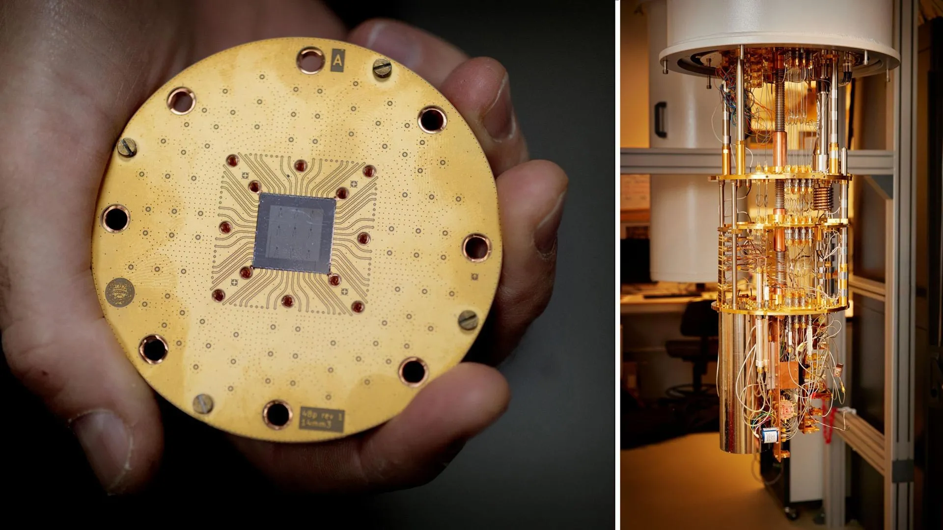
Quantum computers, the next frontier of computation, rely on qubits – the fundamental units of quantum information. These qubits are exquisitely sensitive to their environment and must be maintained at extremely low temperatures, typically in the millikelvin range, to preserve their quantum states and enable computations. The control electronics required to manage these delicate qubits are a significant bottleneck. Current silicon-based control systems are power-hungry and generate substantial heat, forcing them to be physically separated from the qubits themselves. This separation necessitates extensive and complex wiring, which not only complicates the construction of larger quantum computers but also introduces potential signal degradation and performance limitations.
Professor Zhang eloquently articulates the significance of their breakthrough: "Our work introduces a hardware platform that can be integrated alongside quantum processors." This integration is a game-changer. By leveraging the unique carrier dynamics inherent in silicon carbide, the HKU team has engineered circuits that are thousands of times more energy-efficient than conventional electronics. This dramatic reduction in power consumption translates directly into a significantly reduced thermal load on the cryogenic systems. Imagine a quantum computer where the control electronics are not a thermal burden, but an efficient, integral part of the quantum processor. This would allow for denser qubit arrangements, simpler wiring, and ultimately, the construction of much larger and more powerful quantum machines. The implications for accelerating quantum algorithm development and tackling previously intractable problems are immense.
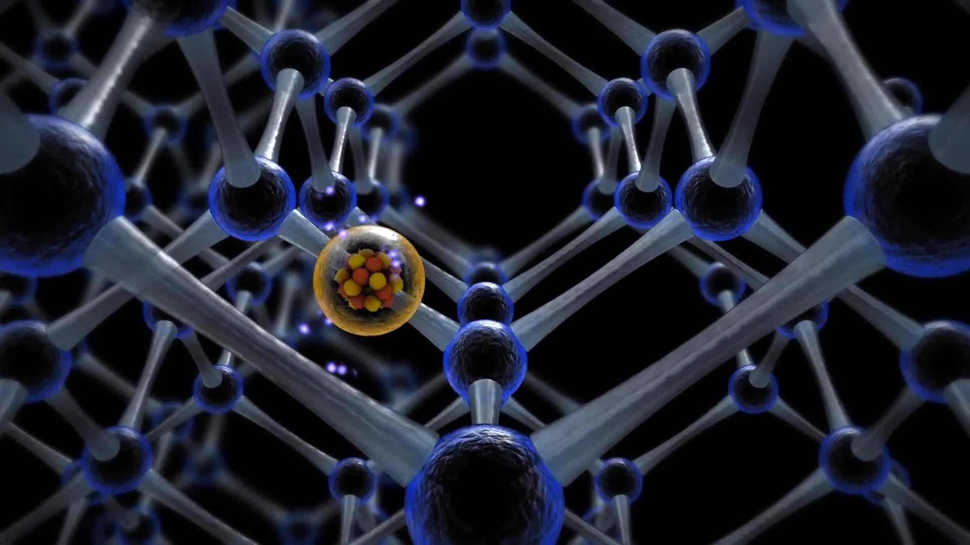
The discovery of SiC MOSFETs’ unique cryogenic behavior was a key finding in this research. The team observed that when these SiC MOSFETs are cooled below 2 Kelvin (K), they exhibit a strong "S-shape" NDR effect. This behavior is not an artifact of heat generation within the device, as is the case with some other NDR mechanisms. Instead, it arises directly from a fundamental property of the silicon carbide material itself: electron-donor impact ionization (EDII). This intrinsic material characteristic makes the observed NDR effect highly stable and consistently reproducible across different manufacturing batches. This reliability is paramount for any technology aiming for widespread adoption, especially in demanding fields like quantum computing and space exploration. The robustness of the SiC material ensures that these cryogenic neuromorphic circuits can be counted on to perform reliably under challenging conditions.
Xin Yang further emphasizes the practicality and scalability of their approach: "This is a robust and scalable approach." The fact that silicon carbide is already a mature and widely used material in high-power electronics for applications like electric vehicles and power grids is a significant advantage. "Because SiC is already used globally in electric vehicles and power grids, we can leverage existing industrial foundries to manufacture these cryogenic chips on 300-mm wafers." This means that the technology is not confined to specialized research labs; it can be integrated into existing semiconductor manufacturing pipelines, accelerating its development and deployment. The ability to produce these specialized cryogenic chips on standard 300-mm wafers promises a cost-effective and high-volume production path, crucial for enabling the widespread adoption of advanced quantum computing and other cryogenic technologies.
The potential of these artificial neurons extends beyond their individual performance. The study also demonstrated a crucial capability: these artificial neurons can be linked together, or "cascaded," into larger networks. This ability to form complex neural architectures at cryogenic temperatures opens up a plethora of advanced functionalities for quantum computing. It could enable sophisticated on-chip, local data processing at the frigid temperatures required for quantum operations, thereby reducing the need for data to be transmitted to warmer classical processors. This is particularly important for critical quantum computing tasks such as quantum error correction, where real-time analysis and correction of errors are essential for maintaining the integrity of quantum computations. Furthermore, it could facilitate real-time quantum control, allowing for more precise and responsive manipulation of qubits.
The applications of this research are not limited to the realm of quantum computing. The circuits’ inherent ability to operate reliably in extremely cold environments makes them exceptionally valuable for deep space exploration. As humanity ventures further into the cosmos, the need for robust electronics that can withstand the harsh conditions of space becomes increasingly critical. Future space missions, whether to the Moon’s frigid polar regions or the icy moons of the outer solar system, could benefit immensely from these cryogenic circuits. Imagine probes equipped with these brain-inspired chips, capable of processing data locally in situ, even in temperatures far below what conventional electronics can endure. This could revolutionize our ability to gather and analyze scientific data from distant and extreme environments.
The findings of this pioneering research were formally published in the esteemed journal Nature Communications, under the title "Cryogenic neuromorphic circuits using gate-controlled negative differential resistance in silicon carbide." This publication signifies the rigorous peer review and validation of their work by the scientific community, cementing its importance and impact on the fields of quantum computing, neuromorphic engineering, and materials science. This breakthrough represents a significant leap forward, paving the way for a new generation of powerful, efficient, and resilient electronic systems that could reshape our technological landscape.