A groundbreaking study, recently published in the prestigious journal Light: Science & Applications, heralds a significant leap forward in this critical area of research. A collaborative effort involving esteemed researchers from Humboldt-Universität zu Berlin, the Leibniz Institute of Photonic Technology, and the University of Stuttgart has yielded a novel type of quantum memory. This innovative memory is constructed from meticulously 3D-nanoprinted structures, ingeniously dubbed "light cages," which are then filled with atomic vapor. By ingeniously co-locating both light and atoms onto a single, integrated chip, the research team has engineered a powerful platform specifically designed for enhanced scalability and effortless integration into the complex architecture of quantum photonic systems.
What Sets These Light Cages Apart: A Paradigm Shift in Quantum Memory Design
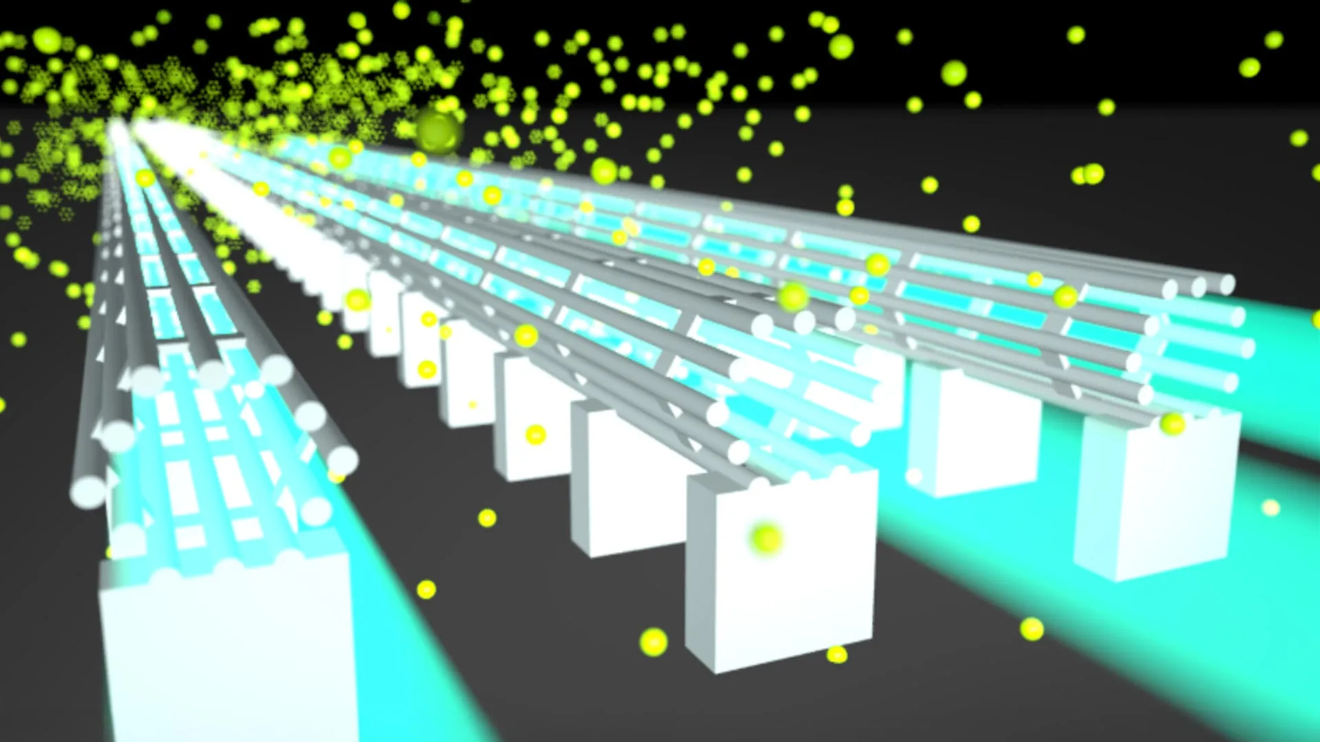
The core innovation lies in the unique design of these "light cages." They are essentially hollow-core waveguides, meticulously engineered to achieve two critical functions simultaneously: to guide light with exceptional precision and to provide unimpeded access to the internal space for atomic vapor. This dual functionality presents a profound advantage over traditional hollow-core fibers, which are notoriously slow and cumbersome to fill with atomic vapor, often requiring months to achieve optimal saturation. In stark contrast, the intrinsically open architecture of the light cages facilitates the rapid diffusion of cesium atoms into the core, dramatically reducing the filling process to a mere matter of days, all while remarkably preserving, and in some cases even enhancing, optical performance.
The fabrication of these intricate structures is achieved through a cutting-edge process known as two-photon polymerization lithography, utilizing readily available commercial 3D printing systems. This advanced technique empowers researchers to directly print highly complex hollow-core waveguides onto silicon chips with an astonishing degree of precision. To safeguard these delicate devices from potentially deleterious chemical reactions with the cesium atoms, the waveguides are subsequently coated with a specialized protective layer. Rigorous testing has confirmed the remarkable long-term stability of these structures, with no observable signs of degradation even after an extended period of five years of continuous operation, a testament to their robust design and material selection.
The research team articulated the significance of their creation, stating, "We created a guiding structure that allows quick diffusion of gases and fluids inside its core, with the versatility and reproducibility provided by the 3D-nanoprinting process. This enables true scalability of this platform, not only for intra-chip fabrication of the waveguides but also inter-chip, for producing multiple chips with the same performance." This statement underscores the dual promise of the technology: both the ability to create complex waveguide networks on a single chip and the capacity to mass-produce identical, high-performance chips.
The Art of Transforming Light into Stored Quantum Information: A Seamless Conversion Process
Within the confines of these precisely engineered light cages, an elegant quantum transduction process unfolds. Incoming light pulses, carrying invaluable quantum information, are efficiently converted into collective excitations of the surrounding atomic vapor. This state represents the storage of quantum information within the atoms. After a predetermined storage duration, precisely controlled by a carefully timed laser pulse, this process is elegantly reversed. The stored quantum state is then converted back into light, released at the exact moment it is required for subsequent operations. In a pivotal experimental demonstration, the researchers showcased their ability to store exceptionally weak light pulses, containing as few as a handful of photons, for durations of several hundred nanoseconds. Their ambitious vision extends this capability even further, with the belief that this methodology can be refined to store single photons for considerably longer periods, potentially extending to many milliseconds.
Another monumental achievement in this research is the successful integration of multiple light cage memories onto a single chip. This chip was then strategically placed within a cesium vapor cell, ensuring a consistent and readily available source of atomic vapor. Crucially, experimental measurements revealed that different light cages, despite being distinct physical structures on the chip, exhibited nearly identical storage performance. This remarkable consistency was observed across two separate devices fabricated on the same chip, a level of uniformity that is absolutely indispensable for the construction of any truly scalable quantum system.
This exceptional reproducibility can be directly attributed to the unparalleled precision inherent in the 3D-nanoprinting process. The researchers meticulously controlled variations, achieving intra-chip discrepancies of less than 2 nanometers and inter-chip differences of under 15 nanometers. Such stringent control over fabrication is not merely an academic curiosity; it is absolutely critical for enabling techniques like spatial multiplexing, a powerful method that could dramatically amplify the number of quantum memories operating in parallel on a single device, thereby boosting overall computational or communication capacity.
Profound Implications for the Future of Quantum Networks and Computing: Bridging the Gap to Practicality
The development of these innovative light cage quantum memories directly addresses several persistent and long-standing challenges that have hindered the advancement of quantum technologies. In the context of quantum repeater networks, these memories are poised to play a pivotal role in synchronizing multiple single photons concurrently, a capability that will significantly enhance the efficiency and reliability of long-distance quantum communication. Furthermore, within the realm of photonic quantum computing, these memories provide the precisely controlled delays that are absolutely essential for implementing feed-forward operations, a critical component of measurement-based quantum computing architectures.
Beyond their technical prowess, the platform distinguishes itself through its remarkable practicality. In sharp contrast to many competing quantum memory technologies that necessitate cryogenic cooling or complex and resource-intensive atom-trapping setups, this system operates comfortably slightly above room temperature. This significantly simplifies deployment and reduces operational costs. Moreover, it offers a superior bandwidth per memory mode, a crucial factor for high-performance applications. The ability to readily produce a multitude of identical quantum memories on a single chip provides a clear and viable pathway towards achieving large-scale quantum photonic integration, a long-sought-after goal in the field.
The inherent flexibility of the fabrication process also opens exciting avenues for future integration. The technology can potentially be seamlessly combined with direct fiber coupling techniques and existing, mature photonic components, facilitating its adoption into current infrastructure. These multifaceted advantages collectively position light cage quantum memories as a formidable contender for shaping the future quantum communication infrastructure.
A Scalable and Promising Path Forward: Illuminating the Quantum Frontier
The ongoing development of light cage quantum memories represents a truly significant milestone in the dynamic field of quantum photonic research. By masterfully merging the sophistication of advanced 3D-nanoprinting techniques with the fundamental principles of quantum optics, the researchers have successfully engineered a system that is both remarkably compact and exceptionally scalable. This breakthrough holds the profound potential to accelerate the arrival of practical, widespread quantum networks and the development of vastly more powerful quantum computers, ushering in a new era of technological innovation.