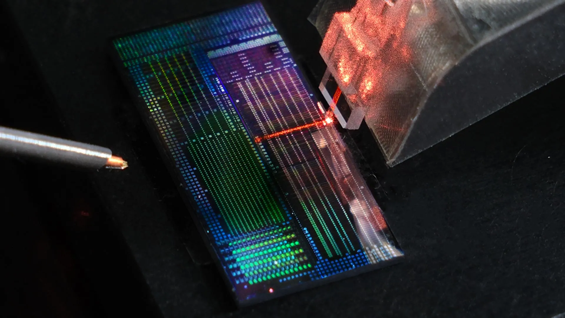
Beyond its astonishingly small dimensions, the manufacturing process of this groundbreaking device is equally transformative. In a departure from the laborious, custom-built laboratory setups that have historically characterized quantum research, the scientists have embraced scalable manufacturing methods. These techniques are remarkably similar to those employed in the mass production of the processors that power our everyday technologies—from the intricate chips in smartphones and computers to the essential components in vehicles and even the humble toaster. This pragmatic, industry-standard approach dramatically enhances the device’s practicality and feasibility for large-scale production.
A Tiny Device Built for Real-World Scale: The Promise of Mass Production
The pioneering research was spearheaded by Jake Freedman, an incoming PhD student within the Department of Electrical, Computer and Energy Engineering, working in close collaboration with Matt Eichenfield, a distinguished professor and the Karl Gustafson Endowed Chair in Quantum Engineering. The team’s efforts were further bolstered by a crucial partnership with scientists from Sandia National Laboratories, including co-senior author Nils Otterstrom. Collectively, they have engineered a device that masterfully integrates diminutive size, exceptional performance, and remarkably low cost, thereby positioning it as an ideal candidate for mass manufacturing.
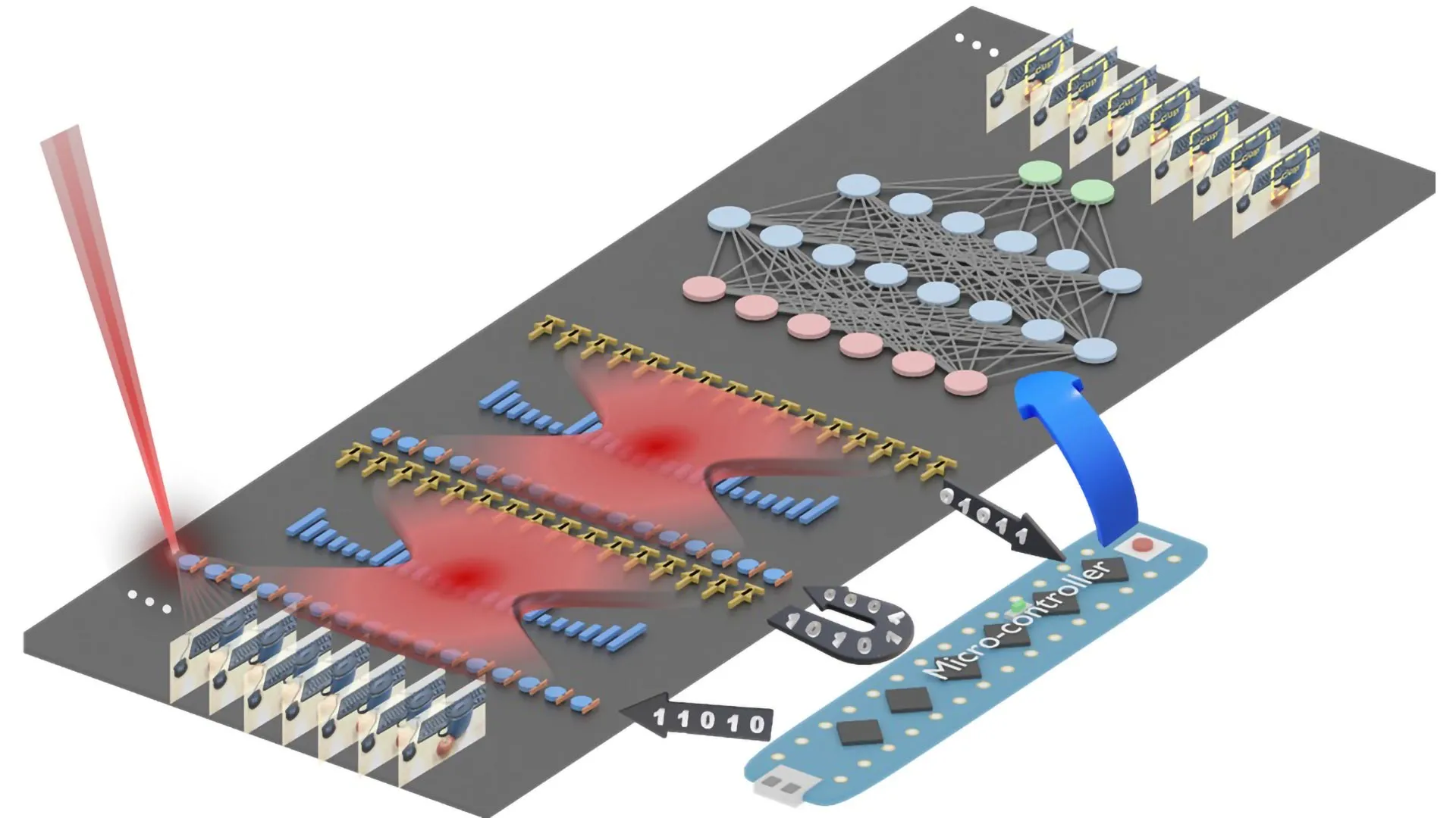
At the core of this innovative technology lies the manipulation of microwave-frequency vibrations, which oscillate at an astonishing rate of billions of times per second. These high-frequency oscillations empower the chip to orchestrate the behavior of laser light with an almost uncanny level of precision. By directly influencing the phase of a laser beam, the device possesses the capability to generate new laser frequencies. Crucially, these newly generated frequencies are both inherently stable and remarkably efficient, a dual characteristic that is paramount for advanced quantum applications. This sophisticated level of control is not confined to quantum computing alone; it is also a cornerstone requirement for the advancement of burgeoning fields such as quantum sensing and quantum networking, promising to unlock new frontiers in scientific discovery and technological innovation.
Why Quantum Computers Need Ultra-Precise Lasers: The Heart of Quantum Computation
The most promising architectures for quantum computing often rely on the intricate manipulation of trapped ions or neutral atoms to serve as qubits. Within these sophisticated systems, each individual atom embodies a qubit, acting as a tiny repository of quantum information. To interact with these delicate qubits and initiate calculations, researchers meticulously direct precisely tuned laser beams towards them. This controlled interaction effectively delivers instructions, enabling the complex quantum computations to unfold. The success of this process hinges on the ability to adjust each laser beam with an extraordinary degree of precision, often requiring accuracy within billionths of a percent.
Jake Freedman elaborates on the significance of this precise frequency control: "Creating new copies of a laser with very exact differences in frequency is one of the most important tools for working with atom- and ion-based quantum computers. But to do that at scale, you need technology that can efficiently generate those new frequencies." Currently, the generation of these precise frequency shifts is achieved through cumbersome, large, table-top devices that demand substantial microwave power. While these systems are adequate for small-scale experimental setups, they are fundamentally impractical for the immense number of optical channels that will be indispensable in future quantum computers.
Professor Eichenfield highlights the logistical challenges of current approaches: "You’re not going to build a quantum computer with 100,000 bulk electro-optic modulators sitting in a warehouse full of optical tables. You need some much more scalable ways to manufacture them that don’t have to be hand-assembled and with long optical paths. While you’re at it, if you can make them all fit on a few small microchips and produce 100 times less heat, you’re much more likely to make it work."
Lower Power Use, Less Heat, More Qubits: A Paradigm Shift in Efficiency
The newly developed device achieves laser frequency shifts through highly efficient phase modulation, a process that consumes approximately 80 times less microwave power compared to many existing commercial modulators. This dramatic reduction in power consumption translates directly into significantly less heat generation. The consequence of reduced heat is a greater density of functionality; more channels can be packed closely together, even onto a single chip, without succumbing to thermal limitations. Collectively, these advantages coalesce to transform the chip into a truly scalable system. It is now capable of orchestrating the precise, delicate interactions that atoms require to perform complex quantum calculations, paving the way for quantum computers with vastly greater computational power.
Built With the Same Technology as Modern Microchips: Leveraging the Power of CMOS
One of the project’s most profound achievements lies in the fact that the device was manufactured entirely within a fabrication facility, or "fab"—the very same type of environment responsible for producing the advanced microelectronics that permeate our modern world. "CMOS fabrication is the most scalable technology humans have ever invented," states Professor Eichenfield. "Every microelectronic chip in every cell phone or computer has billions of essentially identical transistors on it. So, by using CMOS fabrication, in the future, we can produce thousands or even millions of identical versions of our photonic devices, which is exactly what quantum computing will need."
According to Otterstrom, the team’s innovative approach involved taking modulator technologies that were once characterized by their bulkiness, exorbitant cost, and high power demands, and fundamentally redesigning them. The result is a device that is not only significantly smaller and more energy-efficient but also far easier to integrate into complex systems. "We’re helping to push optics into its own ‘transistor revolution,’ moving away from the optical equivalent of vacuum tubes and towards scalable integrated photonic technologies," Otterstrom remarks, drawing a powerful analogy to the historical impact of the transistor on electronics.
Toward Fully Integrated Quantum Photonic Chips: The Next Frontier
The researchers are not resting on their laurels; they are actively engaged in developing fully integrated photonic circuits. This ambitious endeavor aims to consolidate multiple critical functions—including frequency generation, filtering, and pulse shaping—onto a single chip. This integrated approach represents a significant leap forward, moving the field closer to the realization of a complete, self-contained, and operational quantum photonic platform.
The next strategic step for the team involves forging partnerships with leading quantum computing companies. These collaborations will enable them to rigorously test these advanced chips within cutting-edge trapped-ion and trapped-neutral-atom quantum computers. Jake Freedman expresses optimism about the future: "This device is one of the final pieces of the puzzle. We’re getting close to a truly scalable photonic platform capable of controlling very large numbers of qubits." The significant progress made in this project received crucial support from the U.S. Department of Energy, specifically through the Quantum Systems Accelerator program, a distinguished National Quantum Initiative Science Research Center. This collaborative effort underscores the national commitment to advancing quantum technologies, with this tiny chip emerging as a pivotal component in the quest for powerful, scalable quantum computing.