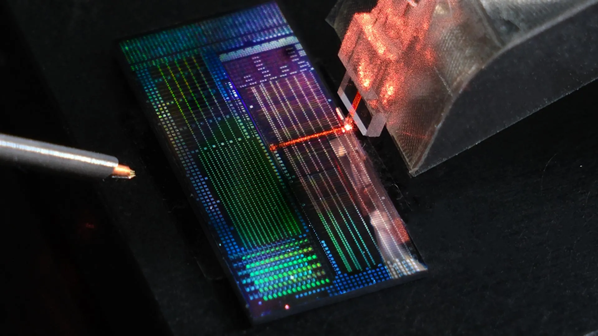
Equally as crucial as its diminutive size is the innovative manufacturing methodology employed for this device. Diverging from the reliance on bespoke, laboratory-bound equipment, the researchers have successfully adopted scalable manufacturing techniques. These methods are remarkably akin to those used in the mass production of processors that power the ubiquitous technologies in our daily lives: computers, smartphones, vehicles, and even common household appliances. Essentially, any device that draws electrical power, from the most sophisticated server to the humble toaster, benefits from this standardized manufacturing paradigm. This strategic choice of production method imbues the device with a profound practicality, paving the way for its efficient and widespread manufacture.
A Tiny Device Built for Real-World Scale
Spearheading this transformative research was Jake Freedman, an aspiring PhD student within the Department of Electrical, Computer and Energy Engineering. He was joined by the insightful leadership of Matt Eichenfield, a distinguished professor and holder of the Karl Gustafson Endowed Chair in Quantum Engineering. The collaborative spirit extended beyond the university, with vital contributions from scientists at Sandia National Laboratories, including co-senior author Nils Otterstrom. Collectively, this synergistic team has engineered a device that masterfully balances diminutive size, exceptional performance, and cost-effectiveness, rendering it eminently suitable for mass production and integration into future technologies.
At the very core of this pioneering technology lies the ingenious manipulation of microwave-frequency vibrations. These vibrations oscillate at astonishing rates, billions of times per second, granting the chip the ability to modulate laser light with an almost unbelievable degree of precision. By directly influencing the phase of a laser beam, the device exhibits the remarkable capacity to generate new laser frequencies. These newly created frequencies are not only stable, ensuring reliability, but also highly efficient, minimizing energy waste. This refined level of control transcends the immediate needs of quantum computing, proving to be a critical requirement for burgeoning fields such as quantum sensing, which demands exquisite sensitivity to environmental signals, and quantum networking, which necessitates the secure and efficient transmission of quantum information.
Why Quantum Computers Need Ultra-Precise Lasers
A significant segment of the most promising quantum computing architectures currently being explored relies on the principles of trapping individual ions or neutral atoms to serve as qubits. In these sophisticated systems, each atom is meticulously isolated and manipulated, effectively acting as a quantum bit capable of storing and processing information. The fundamental mechanism for interacting with these quantum states involves directing precisely tuned laser beams at the atoms. These laser beams act as the communication channel, delivering instructions that enable complex quantum calculations to unfold. For this intricate dance of quantum mechanics to occur flawlessly, each laser beam must be adjusted with an almost unimaginable level of precision. This precision can be as fine as within billionths of a percent of the target frequency, highlighting the extraordinary demands placed on the control mechanisms.
"Creating new copies of a laser with very exact differences in frequency is one of the most important tools for working with atom- and ion-based quantum computers," Freedman elaborated. "But to do that at scale, you need technology that can efficiently generate those new frequencies." The current state of affairs often involves cumbersome, table-top devices that consume substantial amounts of microwave power to achieve these precise frequency shifts. While these systems have proven effective for foundational experiments in controlled laboratory settings, their sheer size, power demands, and lack of scalability render them entirely impractical for the colossal number of optical channels that will be indispensable for future quantum computers, which aim to control thousands or even millions of qubits.
The impracticality of current solutions was underscored by Professor Eichenfield’s candid observation: "You’re not going to build a quantum computer with 100,000 bulk electro-optic modulators sitting in a warehouse full of optical tables. You need some much more scalable ways to manufacture them that don’t have to be hand-assembled and with long optical paths. While you’re at it, if you can make them all fit on a few small microchips and produce 100 times less heat, you’re much more likely to make it work." This statement succinctly encapsulates the formidable engineering challenges that have historically hindered the progress of large-scale quantum computing.
Lower Power Use, Less Heat, More Qubits
The newly developed device directly addresses these limitations by generating laser frequency shifts through highly efficient phase modulation. Critically, it accomplishes this while consuming approximately 80 times less microwave power than many commercially available modulators currently in use. This drastic reduction in power consumption translates directly into a commensurate decrease in heat generation. The implications of less heat are profound: it allows for a far greater density of these optical channels to be packed together, even onto a single, compact microchip. This increased density is a fundamental enabler for the scaling of quantum systems.
When all these advantages are considered in concert, the chip transforms from a mere laboratory curiosity into a truly scalable system. This system possesses the requisite capability to meticulously coordinate the precise interactions between individual atoms, a non-negotiable requirement for them to perform complex quantum calculations. The ability to manage such a large number of precisely controlled atomic qubits is the very essence of building a powerful quantum computer.
Built With the Same Technology as Modern Microchips
One of the most significant and forward-looking achievements of this research project is the complete manufacturing of the device within a fabrication facility, or "fab." This is the very same type of high-tech environment that is responsible for producing the advanced microelectronics that form the backbone of our digital world. The implications of this manufacturing approach are immense.
"CMOS fabrication is the most scalable technology humans have ever invented," Professor Eichenfield asserted, highlighting the profound significance of this choice. He further explained, "Every microelectronic chip in every cell phone or computer has billions of essentially identical transistors on it. So, by using CMOS fabrication, in the future, we can produce thousands or even millions of identical versions of our photonic devices, which is exactly what quantum computing will need." This analogy to the ubiquitous transistors in modern microchips underscores the potential for exponential scaling.
According to Otterstorm, the team embarked on a mission to reimagine modulator technologies that were historically characterized by their bulkiness, exorbitant cost, and significant power consumption. They successfully redesigned these components to be substantially smaller, dramatically more energy-efficient, and considerably easier to integrate into complex systems.
"We’re helping to push optics into its own ‘transistor revolution,’ moving away from the optical equivalent of vacuum tubes and towards scalable integrated photonic technologies," Otterstorm proudly stated. This evocative comparison to the historical "transistor revolution" in electronics signals a paradigm shift in photonic device engineering, moving towards miniaturization, efficiency, and mass-producibility.
Toward Fully Integrated Quantum Photonic Chips
The researchers are not resting on their laurels; they are actively pursuing the development of fully integrated photonic circuits. This ambitious undertaking aims to consolidate multiple critical functions – including frequency generation, filtering, and pulse shaping – onto a single chip. This concentrated effort is a crucial step towards realizing a complete, self-contained, and operational quantum photonic platform.
Looking ahead, the team has concrete plans to forge partnerships with leading quantum computing companies. These collaborations will facilitate the testing of these cutting-edge chips within advanced trapped-ion and trapped-neutral-atom quantum computers. This hands-on validation in real-world quantum computing environments will be instrumental in demonstrating the practical utility and performance of the new technology.
"This device is one of the final pieces of the puzzle," Freedman concluded with optimism. "We’re getting close to a truly scalable photonic platform capable of controlling very large numbers of qubits." This sentiment captures the collective anticipation of the research community as this miniaturized, high-performance optical modulator promises to unlock the next stage of quantum computing development. The project’s vital progress was made possible through the generous support of the U.S. Department of Energy, specifically through the Quantum Systems Accelerator program, a distinguished National Quantum Initiative Science Research Center.