The significance of this breakthrough extends far beyond its diminutive size; the methodology employed in its creation is equally, if not more, transformative. Eschewing the need for custom-built, labor-intensive laboratory equipment, the researchers have ingeniously leveraged scalable manufacturing techniques. These are the very same sophisticated processes that underpin the mass production of the ubiquitous processors found in our computers, smartphones, vehicles, and an array of household appliances – in essence, any technology that relies on electrical power, from the most advanced supercomputers to the humble toaster. This strategic adoption of established, high-volume manufacturing paradigms renders the device eminently practical for widespread, large-scale production.
A Miniature Marvel Engineered for Real-World Scalability
The pioneering research was spearheaded by Jake Freedman, an incoming PhD student within the Department of Electrical, Computer and Energy Engineering, working in close collaboration with Matt Eichenfield, a distinguished professor and holder of the Karl Gustafson Endowed Chair in Quantum Engineering. The collaborative spirit of the project also extended to esteemed scientists from Sandia National Laboratories, notably co-senior author Nils Otterstrom. United by a shared vision, this formidable team has engineered a device that masterfully integrates diminutive size, exceptional performance, and cost-effectiveness, positioning it as an ideal candidate for mass manufacturing.
At the very core of this revolutionary technology lie microwave-frequency vibrations, oscillating at an astonishing rate of billions of cycles per second. These high-frequency oscillations imbue the chip with the remarkable ability to manipulate laser light with an unparalleled degree of precision. By exerting direct control over the phase of a laser beam, the device possesses the power to generate new laser frequencies that are both exceptionally stable and remarkably efficient. This sophisticated level of control is not merely a desirable attribute for quantum computing; it is a critical prerequisite for the advancement of burgeoning fields such as quantum sensing and quantum networking.
The Indispensable Role of Ultra-Precise Lasers in Quantum Computing
Among the most promising architectures for quantum computing are those that employ trapped ions or trapped neutral atoms as the physical substrate for storing quantum information. In these intricate systems, each individual atom functions as a qubit, holding a quantum state. The intricate dance of quantum computation is orchestrated by directing meticulously tuned laser beams towards these atoms, effectively issuing precise instructions that enable complex calculations to unfold. For this process to yield accurate results, each laser must be adjusted with extraordinary precision, often to within an infinitesimal margin of error, measured in billionths of a percent.
"The ability to generate new copies of a laser with extremely precise differences in frequency is one of the most critical tools for working with atom- and ion-based quantum computers," elucidated Freedman. "However, to achieve this capability at scale, one requires technology that can efficiently generate those new frequencies."
Currently, the generation of these precise frequency shifts is accomplished through the use of cumbersome, large, table-top devices that demand significant microwave power. While these systems may suffice for small-scale experimental setups, they are fundamentally impractical for the colossal number of optical channels that will be indispensable for the quantum computers of the future.
"The prospect of constructing a quantum computer populated with 100,000 bulk electro-optic modulators, occupying an entire warehouse filled with optical tables, is simply not feasible," stated Eichenfield. "We urgently need far more scalable manufacturing methods that eliminate the necessity for manual assembly and lengthy optical paths. Furthermore, if we can miniaturize these components to fit onto a few small microchips and simultaneously reduce their heat output by a factor of 100, the likelihood of achieving a functional quantum computer increases dramatically."
Reduced Power Consumption, Minimized Heat, and Amplified Qubit Capacity
The newly developed device achieves laser frequency shifts through highly efficient phase modulation, while concurrently consuming approximately 80 times less microwave power compared to many existing commercial modulators. This drastic reduction in power consumption translates directly into significantly less heat generation. This, in turn, enables a greater density of optical channels to be packed into a confined space, even allowing for their integration onto a single chip. Collectively, these synergistic advantages transform the chip into a truly scalable system, capable of orchestrating the precise interactions between atoms that are fundamental to the execution of quantum computations.
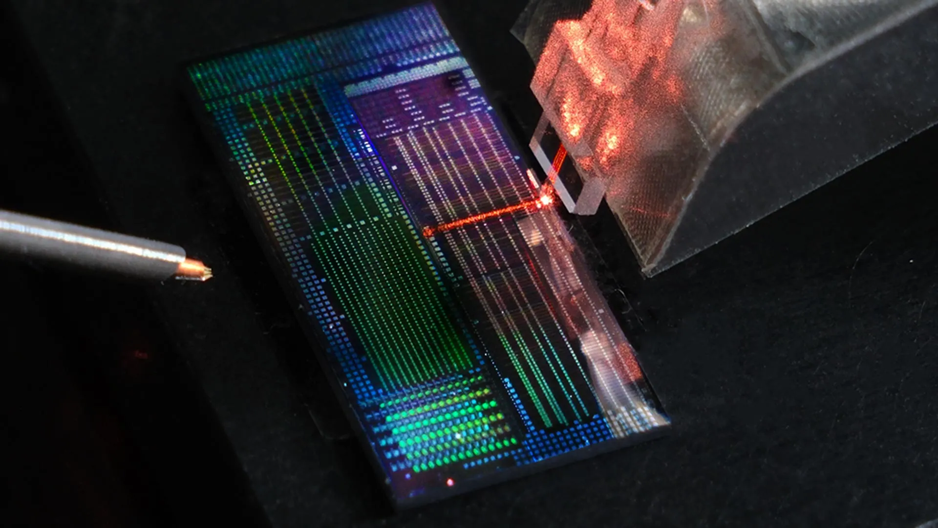
Constructed Using the Same Advanced Technology as Modern Microchips
One of the project’s most profound achievements lies in the fact that the device was manufactured entirely within a fabrication facility, or "fab," which is precisely the same type of environment utilized for the production of advanced microelectronics.
"CMOS fabrication represents the most scalable technology that humanity has ever conceived," asserted Eichenfield. "Every microelectronic chip found in virtually every cell phone or computer is populated with billions of essentially identical transistors. Therefore, by harnessing the power of CMOS fabrication, we can, in the future, produce thousands, if not millions, of identical versions of our photonic devices, which is precisely what the advancement of quantum computing necessitates."
According to Otterstrom, the research team has successfully reimagined modulator technologies that were once characterized by their bulkiness, prohibitive cost, and substantial power demands, redesigning them to be significantly smaller, more energy-efficient, and considerably easier to integrate.
"We are instrumental in propelling optics into its own ‘transistor revolution,’ marking a decisive departure from the optical equivalent of vacuum tubes and heralding the advent of scalable integrated photonic technologies," remarked Otterstorm.
Paving the Way for Fully Integrated Quantum Photonic Chips
The researchers are currently engaged in the ambitious endeavor of developing fully integrated photonic circuits. These advanced circuits will seamlessly combine frequency generation, filtering, and pulse shaping capabilities onto a single, unified chip. This concerted effort is progressively advancing the field towards the realization of a complete, fully operational quantum photonic platform.
In the immediate future, the team intends to forge strategic partnerships with leading quantum computing companies. These collaborations will facilitate the rigorous testing of these innovative chips within state-of-the-art trapped-ion and trapped-neutral-atom quantum computers.
"This device represents one of the final, crucial pieces of the puzzle," Freedman stated with evident optimism. "We are rapidly approaching the development of a truly scalable photonic platform that possesses the capacity to precisely control an exceptionally large number of qubits."
This transformative project received crucial financial and scientific support from the U.S. Department of Energy, channeled through the Quantum Systems Accelerator program, a distinguished National Quantum Initiative Science Research Center.