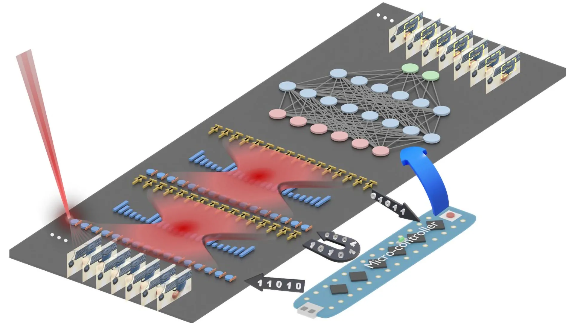
In a significant leap forward for artificial intelligence hardware and a potent boost to American semiconductor innovation, a collaborative team of engineers from Stanford University, Carnegie Mellon University, the University of Pennsylvania, and the Massachusetts Institute of Technology, working in tandem with SkyWater Technology – the nation’s largest exclusively U.S.-based pure-play semiconductor foundry – has unveiled a groundbreaking new multilayer computer chip. This revolutionary architecture, unlike the predominantly flat, two-dimensional chips that currently dominate the market, is engineered to stack vertically, mimicking the structure of a skyscraper. Ultra-thin components are meticulously layered like floors, interconnected by a sophisticated network of vertical wiring that functions akin to high-speed elevators, capable of ferrying vast quantities of data with unprecedented speed and efficiency. The prototype boasts a record-breaking number of vertical connections and an intricately woven layout that strategically positions memory and computing units in close proximity. This design innovation directly addresses and circumvents the debilitating slowdowns that have long plagued the progress of flat chips, a critical limitation in the ever-increasing demands of modern AI. In rigorous hardware tests and simulations, this novel 3D chip has demonstrated performance improvements of approximately an order of magnitude when compared to its 2D counterparts. While experimental 3D chips have emerged from academic laboratories in the past, this marks the first instance where such a chip has delivered tangible, significant performance enhancements and, crucially, has been successfully produced within a commercial foundry setting.
Subhasish Mitra, the William E. Ayer Professor in Electrical Engineering and professor of computer science at Stanford University and principal investigator for the seminal paper detailing this chip, presented at the 71st Annual IEEE International Electron Devices Meeting (IEDM), hailed this development as the dawn of a "new era of chip production and innovation." He further emphasized, "Breakthroughs like this are how we get to the 1,000-fold hardware performance improvements future AI systems will demand."
The Achilles’ Heel of Flat Chips in the Age of AI
The burgeoning field of artificial intelligence, particularly with the advent of sophisticated large language models like ChatGPT and Claude, is characterized by an insatiable appetite for data. These powerful AI systems are constantly engaged in the strenuous task of shuttling immense volumes of information back and forth between memory units, which store critical data, and the processing cores, responsible for its computation.
In the realm of conventional 2D chips, this data transfer process is inherently hampered. Because all components reside on a single surface, memory is often limited in capacity and spread out across the chip. This spatial distribution necessitates that data traverse long, often congested pathways, creating a bottleneck. The computing units, capable of executing operations at remarkable speeds, frequently find themselves waiting idly for data to arrive, as the chip’s ability to supply it is outpaced. This frustrating phenomenon is widely known in engineering circles as the "memory wall," a critical impediment where processing power is rendered ineffective by the limitations of data delivery and nearby memory access.
For years, the semiconductor industry’s primary strategy to push back against this memory wall has been through the relentless shrinking of transistors – the microscopic switches that perform computations and store data – thereby packing more of them onto each chip. However, researchers are increasingly recognizing that this approach is approaching its fundamental physical limits, a concept often referred to as the "miniaturization wall."
The innovative 3D chip design directly confronts and aims to surmount both of these formidable walls by fundamentally altering the chip’s physical dimension: building upward. Tathagata Srimani, assistant professor of electrical and computer engineering at Carnegie Mellon University and the paper’s senior author, who initiated this groundbreaking work as a postdoctoral fellow under Mitra’s guidance, eloquently explained the paradigm shift: "By integrating memory and computation vertically, we can move a lot more information much quicker, just as the elevator banks in a high-rise let many residents travel between floors at once."
Robert M. Radway, assistant professor of electrical and systems engineering at the University of Pennsylvania and a co-author of the study, articulated the severity of the challenge: "The memory wall and the miniaturization wall form a deadly combination." He continued, "We attacked it head-on by tightly integrating memory and logic and then building upward at extremely high density. It’s like the Manhattan of computing – we can fit more people in less space."
The Manufacturing Marvel: Crafting the Monolithic 3D Chip
Previous attempts at creating 3D chips often adopted a more straightforward approach: stacking pre-fabricated, separate chips. While this method offers some advantages, the connections between these stacked layers are typically less refined, limited in number, and prone to becoming significant bottlenecks in data flow.
This research team, however, pursued a fundamentally different and more advanced methodology. Instead of fabricating individual chips and then bonding them together, they meticulously build each new layer directly atop the preceding one, employing a continuous, integrated manufacturing process. This technique, known as "monolithic" 3D integration, is executed at temperatures sufficiently low to prevent any damage to the circuitry already established in the underlying layers. This critical capability allows for an unprecedented density of stacked layers and the creation of vastly more numerous and efficient connections between them.
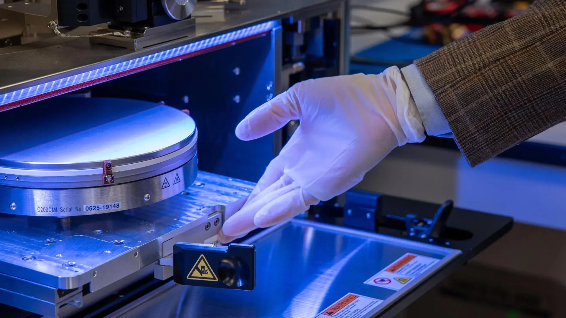
A particularly noteworthy aspect of this achievement, according to the researchers, is the fact that the entire fabrication process was successfully conducted within a domestic, commercial silicon foundry. Mark Nelson, vice president of technology development operations at SkyWater Technology and a co-author of the study, underscored the magnitude of this accomplishment: "Turning a cutting-edge academic concept into something a commercial fab can build is an enormous challenge." He further elaborated, "This shows that these advanced architectures aren’t just possible in the lab – they can be produced domestically, at scale, which is what America needs to stay at the forefront of semiconductor innovation."
Performance Triumphs and the Horizon of AI Hardware Evolution
Initial hardware tests have already yielded compelling results, with the prototype chip outperforming comparable 2D chips by approximately fourfold. The team’s sophisticated simulations project even more dramatic performance gains as the design scales vertically, incorporating additional stacked layers of memory and compute units. Projections indicate that with further tiers, these models could achieve up to a twelvefold improvement on realistic AI workloads, including those derived from Meta’s widely recognized open-source LLaMA model.
Beyond immediate performance enhancements, the researchers highlight a significant long-term benefit. The proposed architecture presents a viable pathway to achieving a staggering 100 to 1,000-fold improvement in the Energy Delay Product (EDP). EDP is a crucial metric that quantifies the combined efficiency of a chip’s speed and its energy consumption. By drastically reducing the distance data must travel and introducing a multitude of vertical pathways for data movement, the chip can simultaneously increase throughput – the amount of work done per unit of time – while decreasing the energy expended per operation, a dual objective that has remained elusive with conventional flat chip designs.
The significance of this research extends beyond mere speed improvements. By demonstrating the feasibility of producing monolithic 3D chips within the United States, the team has effectively laid out a blueprint for a new era of domestic hardware innovation. This advancement positions the U.S. to lead in the design and manufacturing of the most advanced chips on its own soil.
Furthermore, the transition to vertical, monolithic 3D integration necessitates a new generation of engineers proficient in these sophisticated methods. This parallels the transformative impact of the integrated circuit boom in the 1980s, which was propelled by students acquiring expertise in chip design and fabrication within U.S. laboratories. Through active collaborations and robust funding initiatives, such as the Microelectronics Commons California-Pacific-Northwest AI Hardware Hub (Northwest-AI-Hub), students and researchers are already being cultivated to drive the future of American semiconductor innovation.
H.-S. Philip Wong, the Willard R. and Inez Kerr Bell Professor in the Stanford School of Engineering and principal investigator of the Northwest-AI-Hub, articulated the dual importance of this breakthrough: "Breakthroughs like this are of course about performance," he stated. "But they’re also about capability. If we can build advanced 3D chips, we can innovate faster, respond faster, and shape the future of AI hardware."
This landmark study was a collective effort undertaken at the Stanford University School of Engineering, Carnegie Mellon University College of Engineering, the University of Pennsylvania School of Engineering and Applied Science, and the Massachusetts Institute of Technology. All fabrication processes were meticulously completed at SkyWater Technology’s Foundry located in Bloomington, Minnesota. The research received vital support from a consortium of esteemed organizations, including the Defense Advanced Research Projects Agency, the U.S. National Science Foundation Graduate Research Fellowship Program, Samsung, the Stanford Precourt Institute for Energy, the Stanford SystemX Alliance, the Department of War’s Microelectronics Commons AI Hardware Hub, the U.S. Department of Energy, and the National Science Foundation’s Future of Semiconductors Program (grant number 2425218).
Additional Stanford co-authors contributing to this pivotal research include Suhyeong Choi, Samuel Dayo, Andrew Bechdolt, Shengman Li, Dennis T. Rich, and R.H. Yang. Further esteemed authors also contributed from Carnegie Mellon University and the Massachusetts Institute of Technology, underscoring the truly collaborative and interdisciplinary nature of this significant advancement.