Unlike the predominantly flat, two-dimensional (2D) chips that characterize most of today’s computing landscape, this pioneering prototype is engineered to ascend vertically. Imagine a towering edifice where ultra-thin components are meticulously stacked, akin to floors in a skyscraper. This vertical construction is complemented by an intricate network of vertical wiring, functioning as a multitude of high-speed elevators, capable of whisking enormous volumes of data across the chip with remarkable alacrity. The design boasts a record-breaking number of vertical connections, meticulously interwoven with a densely packed layout that strategically positions memory and computing units in close proximity. This spatial optimization is crucial, as it effectively circumvents the debilitating slowdowns that have historically constrained the progress of flat chip designs. In rigorous hardware tests and sophisticated simulations, this novel 3D chip has demonstrated performance that eclipses its 2D counterparts by approximately an order of magnitude, a testament to its revolutionary design.
While the concept of experimental 3D chips has been explored in academic laboratories for some time, this development marks a significant milestone. The research team asserts that this is the first instance where a 3D chip has delivered tangible and substantial performance improvements and, crucially, has been successfully produced within a commercial foundry. "This opens the door to a new era of chip production and innovation," declared Subhasish Mitra, the William E. Ayer Professor in Electrical Engineering and a professor of computer science at Stanford University, who also serves as the principal investigator of a seminal paper detailing this chip, presented at the 71st Annual IEEE International Electron Devices Meeting (IEDM). He further emphasized, "Breakthroughs like this are how we get to the 1,000-fold hardware performance improvements future AI systems will demand."
The inherent limitations of flat chips in powering modern AI
The burgeoning field of artificial intelligence, exemplified by sophisticated models like ChatGPT and Claude, is characterized by its insatiable appetite for data. These large language models constantly engage in the arduous task of shuttling colossal volumes of data between memory, the repository of information, and the computing units, the engines that process it.
In conventional 2D chips, where all components reside on a single plane, memory is inherently limited and dispersed. This geographical separation forces data to navigate through a constrained number of long, congested pathways. Consequently, the processing units, capable of executing computations at blistering speeds, often find themselves waiting idly, their potential stifled by the chip’s inability to supply data quickly enough. The memory itself is also not situated close enough to the computing elements, leading to a constant bottleneck. This pervasive issue, known as the "memory wall," signifies a critical juncture where processing speed outpaces the chip’s capacity to deliver the necessary data.
For years, chip manufacturers have strived to push back against this memory wall by relentlessly shrinking transistors – the microscopic switches responsible for both computation and data storage – and cramming ever-increasing numbers of them onto each chip. However, researchers are increasingly vocal about the fact that this approach is rapidly approaching its fundamental physical limitations, often referred to as the "miniaturization wall."
The innovative design presented by this research team directly confronts and aims to transcend both of these formidable barriers by embracing verticality. "By integrating memory and computation vertically, we can move a lot more information much quicker, just as the elevator banks in a high-rise let many residents travel between floors at once," explained Tathagata Srimani, an assistant professor of electrical and computer engineering at Carnegie Mellon University and the paper’s senior author. Srimani initiated this groundbreaking work as a postdoctoral fellow under the guidance of Professor Mitra.
Robert M. Radway, an assistant professor of electrical and systems engineering at the University of Pennsylvania and a co-author of the study, underscored the severity of the challenge: "The memory wall and the miniaturization wall form a deadly combination. We attacked it head-on by tightly integrating memory and logic and then building upward at extremely high density. It’s like the Manhattan of computing – we can fit more people in less space." This analogy vividly illustrates the compact and efficient nature of the 3D design, akin to a bustling metropolis where verticality maximizes utility.
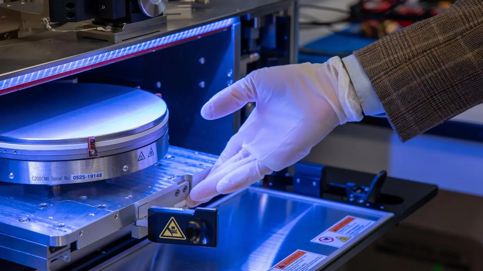
The sophisticated manufacturing process of the Monolithic 3D Chip
Previous endeavors in developing 3D chips have often adopted a more straightforward approach: stacking pre-fabricated separate chips. While this method can offer some advantages, the inter-layer connections in such designs are frequently suboptimal, characterized by limitations in number and potential bottlenecks that impede data flow.
The research team, however, has pioneered a fundamentally different methodology. Instead of fabricating individual chips and subsequently bonding them together, they meticulously construct each new layer directly atop the preceding one, executing this process in a single, continuous manufacturing flow. This advanced technique, termed "monolithic" 3D integration, employs temperatures that are sufficiently low to avoid any detrimental impact on the circuitry already established in the underlying layers. This critical capability enables the dense stacking of layers and facilitates the creation of a vastly greater number of connections between them.
A pivotal aspect highlighted by the researchers is that the entire manufacturing process was executed within a domestic commercial silicon foundry. "Turning a cutting-edge academic concept into something a commercial fab can build is an enormous challenge," acknowledged co-author Mark Nelson, vice president of technology development operations at SkyWater Technology. He further stated, "This shows that these advanced architectures aren’t just possible in the lab – they can be produced domestically, at scale, which is what America needs to stay at the forefront of semiconductor innovation." This underscores the vital national security and economic implications of the achievement, demonstrating that advanced chip manufacturing can be sustained within the United States.
Tangible performance gains and the future trajectory of AI hardware
In initial hardware evaluations, the prototype chip demonstrated performance approximately four times superior to comparable 2D chips. Furthermore, the team’s sophisticated simulations indicate that these performance gains are poised to escalate significantly as the design matures, with taller structures incorporating more stacked layers of memory and compute. Projections suggest that with additional tiers, these models could achieve an impressive twelve-fold improvement on real-world AI workloads, including those derived from Meta’s open-source LLaMA model.
Beyond immediate performance enhancements, the researchers point to a more profound, long-term payoff. They posit that this architecture provides a viable pathway to achieving 100- to 1,000-fold improvements in the Energy Delay Product (EDP). EDP is a crucial metric that encapsulates both the speed of computation and its energy efficiency. By drastically reducing the distances data must traverse and augmenting the number of vertical pathways for data movement, the chip can simultaneously boost throughput and decrease the energy consumed per operation – a combination that has proven exceptionally elusive with conventional flat chip designs.
The significance of this work extends beyond mere performance metrics. By successfully demonstrating the feasibility of manufacturing monolithic 3D chips within the United States, the researchers are providing a compelling blueprint for a new era of domestic hardware innovation. This heralds an era where the most advanced chips can be conceived, designed, and manufactured on American soil, bolstering national competitiveness and technological leadership.
Moreover, the transition to vertical, monolithic 3D integration necessitates the cultivation of a new generation of engineers proficient in these advanced methodologies. This mirrors the transformative impact of the integrated circuit boom in the 1980s, which was propelled by students acquiring expertise in chip design and fabrication within U.S. laboratories. Through proactive collaborations and dedicated funding initiatives, such as the Microelectronics Commons California-Pacific-Northwest AI Hardware Hub (Northwest-AI-Hub), students and researchers are already being meticulously prepared to propel American semiconductor innovation forward.
"Breakthroughs like this are of course about performance," observed H.-S. Philip Wong, the Willard R. and Inez Kerr Bell Professor in the Stanford School of Engineering and principal investigator of the Northwest-AI-Hub. He added, "But they’re also about capability. If we can build advanced 3D chips, we can innovate faster, respond faster, and shape the future of AI hardware." This perspective emphasizes the strategic imperative of developing these advanced capabilities, not just for immediate gains, but for long-term technological sovereignty and the ability to dictate the future direction of AI.
This landmark study was a collaborative effort undertaken at the Stanford University School of Engineering, Carnegie Mellon University College of Engineering, the University of Pennsylvania School of Engineering and Applied Science, and the Massachusetts Institute of Technology. All fabrication processes were meticulously completed at SkyWater Technology’s Bloomington, Minnesota, Foundry. The research received crucial support from a diverse range of esteemed organizations, including the Defense Advanced Research Projects Agency, the U.S. National Science Foundation Graduate Research Fellowship Program, Samsung, the Stanford Precourt Institute for Energy, the Stanford SystemX Alliance, the Department of War’s Microelectronics Commons AI Hardware Hub, the U.S. Department of Energy, and the National Science Foundation’s Future of Semiconductors Program (under grant number 2425218). Additional Stanford co-authors contributing to this significant research include Suhyeong Choi, Samuel Dayo, Andrew Bechdolt, Shengman Li, Dennis T. Rich, and R.H. Yang, with further contributions from researchers at Carnegie Mellon University and the Massachusetts Institute of Technology, solidifying the truly interdisciplinary and collaborative nature of this monumental achievement.