At its core, the new prototype diverges sharply from the predominantly flat, two-dimensional (2D) chips that characterize current technology. Instead, this design is engineered to ascend vertically, meticulously stacking ultra-thin components akin to floors in a skyscraper. This architectural paradigm is complemented by an intricate network of vertical wiring, functioning as a multitude of high-speed elevators designed to transport vast quantities of data with unprecedented alacrity. The chip boasts a record-setting number of vertical interconnections, coupled with a tightly integrated layout that strategically positions memory and computing units in close proximity. This proximity is crucial, as it effectively circumvents the data transfer slowdowns that have historically constrained the performance of flat chip designs. In rigorous hardware tests and extensive simulations, this pioneering 3D chip has demonstrated performance improvements that are approximately an order of magnitude greater than its 2D counterparts.
While experimental 3D chips have been developed in academic settings previously, the team asserts that this marks the first instance where a 3D chip has delivered tangible, significant performance enhancements and, critically, has been manufactured within a commercial foundry. "This opens the door to a new era of chip production and innovation," declared Subhasish Mitra, the William E. Ayer Professor in Electrical Engineering and professor of computer science at Stanford University, and the principal investigator behind a new paper detailing the chip, which was presented at the 71st Annual IEEE International Electron Devices Meeting (IEDM). He further emphasized, "Breakthroughs like this are how we get to the 1,000-fold hardware performance improvements future AI systems will demand."
The Achilles’ Heel of Flat Chips in the Age of Modern AI
The insatiable hunger for data processing power exhibited by large AI models, such as ChatGPT and Claude, necessitates the constant and rapid shuttling of enormous data volumes between memory units, which store information, and the computing units responsible for its processing.
Within the confines of conventional 2D chips, where all components reside on a single plane, memory capacity is inherently limited and often dispersed. This spatial constraint forces data to traverse lengthy, congested pathways, creating a bottleneck. The computing elements within these chips possess the capability to operate at speeds far exceeding the rate at which data can be supplied. Furthermore, the chip struggles to maintain sufficient memory in close proximity to these computing units. The inevitable consequence is a pervasive state of waiting, where processing capabilities are underutilized due to data starvation. Engineers have aptly termed this phenomenon the "memory wall," a critical juncture where processing speed outpaces the chip’s ability to deliver the necessary data.
For many years, the semiconductor industry attempted to surmount the memory wall by relentlessly shrinking transistors—the fundamental switches that execute computations and store data—and by densely packing ever-increasing numbers of them onto each chip. However, researchers now contend that this approach is rapidly approaching fundamental physical limitations, often referred to as the "miniaturization wall."
The innovative design presented by this research team endeavors to transcend both these formidable barriers by adopting a vertical, three-dimensional construction strategy. "By integrating memory and computation vertically, we can move a lot more information much quicker, just as the elevator banks in a high-rise let many residents travel between floors at once," explained Tathagata Srimani, assistant professor of electrical and computer engineering at Carnegie Mellon University and the paper’s senior author, who initiated this work as a postdoctoral fellow under Mitra’s guidance.
Robert M. Radway, assistant professor of electrical and systems engineering at the University of Pennsylvania and a co-author of the study, articulated the severity of the challenge: "The memory wall and the miniaturization wall form a deadly combination. We attacked it head-on by tightly integrating memory and logic and then building upward at extremely high density. It’s like the Manhattan of computing — we can fit more people in less space."
The Manufacturing Prowess of the Monolithic 3D Chip
Many prior attempts at developing 3D chips have adopted a more straightforward approach, involving the stacking of pre-fabricated individual chips. While this method offers some advantages, the interconnections between these stacked layers are often suboptimal, limited in number, and prone to becoming significant performance bottlenecks.
The approach taken by this research consortium is fundamentally different. Rather than fabricating separate chips and then bonding them together, the team meticulously constructs each new layer directly atop the preceding one in a continuous, uninterrupted manufacturing flow. This technique, known as "monolithic" 3D integration, is enabled by the use of processing temperatures sufficiently low to prevent any damage to the circuitry already established in the lower layers. This critical capability allows for significantly tighter stacking of layers and the creation of a far greater density of interconnections between them.
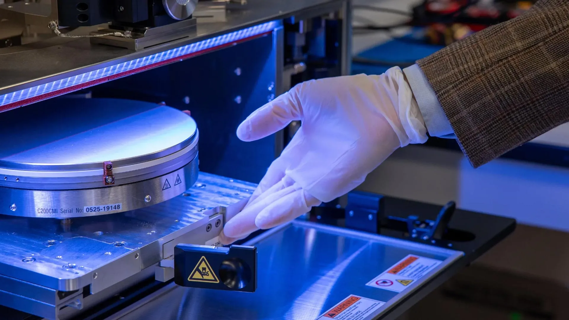
A particularly salient point highlighted by the researchers is the fact that the entire manufacturing process was executed within a domestic commercial silicon foundry. "Turning a cutting-edge academic concept into something a commercial fab can build is an enormous challenge," stated co-author Mark Nelson, vice president of technology development operations at SkyWater Technology. He further emphasized the significance of this achievement: "This shows that these advanced architectures aren’t just possible in the lab — they can be produced domestically, at scale, which is what America needs to stay at the forefront of semiconductor innovation."
Tangible Performance Gains and the Future Trajectory of AI Hardware
Initial hardware tests have revealed that the prototype chip outperforms comparable 2D chips by approximately fourfold. Moreover, the team’s sophisticated simulations project even more substantial performance gains as the design is scaled vertically, incorporating additional stacked layers of memory and compute. With further tiers of integration, simulations indicate potential improvements of up to twelvefold on real-world AI workloads, including those derived from Meta’s widely recognized open-source LLaMA model.
Beyond these immediate performance enhancements, the researchers also point to a significant long-term benefit. They posit that this architecture provides a viable pathway to achieving 100- to 1,000-fold improvements in the energy delay product (EDP), a crucial metric that quantifies the combined efficiency of speed and energy consumption. By drastically reducing the distances data must traverse and introducing a multitude of vertical pathways for data movement, the chip can simultaneously boost throughput and decrease the energy required per operation—a synergistic outcome that has proven exceptionally elusive with conventional flat chip designs.
The significance of this work extends beyond mere performance metrics. By successfully demonstrating that monolithic 3D chips can be manufactured within the United States, the team argues that this achievement lays the groundwork for a new era of domestic hardware innovation, where the most advanced semiconductor technologies can be conceived and produced on American soil.
Furthermore, the transition to vertical, monolithic 3D integration necessitates the cultivation of a new generation of engineers proficient in these advanced methodologies. This mirrors the trajectory of the integrated circuit boom in the 1980s, which was propelled by students acquiring expertise in chip design and fabrication within U.S. laboratories. Through concerted collaborations and strategic funding initiatives, such as those spearheaded by the Microelectronics Commons California-Pacific-Northwest AI Hardware Hub (Northwest-AI-Hub), students and researchers are actively being prepared to drive forward American semiconductor innovation.
"Breakthroughs like this are of course about performance," remarked H.-S. Philip Wong, the Willard R. and Inez Kerr Bell Professor in the Stanford School of Engineering and principal investigator of the Northwest-AI-Hub. "But they’re also about capability. If we can build advanced 3D chips, we can innovate faster, respond faster, and shape the future of AI hardware."
The foundational research for this project was conducted across the Stanford University School of Engineering, Carnegie Mellon University College of Engineering, the University of Pennsylvania School of Engineering and Applied Science, and the Massachusetts Institute of Technology. All fabrication processes were expertly carried out at SkyWater Technology’s Bloomington, Minnesota, Foundry. The project received vital support from a consortium of esteemed organizations, including the Defense Advanced Research Projects Agency, the U.S. National Science Foundation Graduate Research Fellowship Program, Samsung, the Stanford Precourt Institute for Energy, the Stanford SystemX Alliance, the Department of War’s Microelectronics Commons AI Hardware Hub, the U.S. Department of Energy, and the National Science Foundation’s Future of Semiconductors Program (grant number 2425218). Additional contributing authors from Stanford include Suhyeong Choi, Samuel Dayo, Andrew Bechdolt, Shengman Li, Dennis T. Rich, and R.H. Yang, with further contributions from researchers at Carnegie Mellon University and the Massachusetts Institute of Technology.