At the heart of this breakthrough lies a radical departure from the conventional, predominantly flat, two-dimensional (2D) design of most contemporary chips. The newly developed prototype is engineered to ascend vertically, stacking ultra-thin components like floors in a towering edifice. This three-dimensional (3D) construction is complemented by an intricate network of vertical wiring, functioning as a multitude of high-speed elevators designed to transport vast quantities of data with unprecedented rapidity. The chip boasts a record-breaking density of vertical connections and a meticulously interwoven layout that strategically positions memory and computing units in close proximity. This proximity is crucial, as it effectively circumvents the performance bottlenecks that have long hampered the progress of flat chips. In rigorous hardware tests and advanced simulations, this novel 3D chip has demonstrated performance gains that are approximately an order of magnitude superior to its 2D counterparts.
While the concept of 3D chips is not entirely new, with prior experimental prototypes emerging from academic laboratories, this particular development marks a significant milestone. It is the first time such a design has not only delivered demonstrable performance improvements but has also been successfully fabricated within a commercial foundry. "This opens the door to a new era of chip production and innovation," declared Subhasish Mitra, the William E. Ayer Professor in Electrical Engineering and professor of computer science at Stanford University, and the principal investigator of the research. His insights were presented in a new paper detailing the chip at the 71st Annual IEEE International Electron Devices Meeting (IEDM). Professor Mitra further emphasized the transformative potential of such advancements, stating, "Breakthroughs like this are how we get to the 1,000-fold hardware performance improvements future AI systems will demand."
The Achilles’ Heel of Flat Chips in the Age of Modern AI
The insatiable appetite for data exhibited by large AI models, exemplified by systems like ChatGPT and Claude, necessitates the constant and rapid shuttling of enormous data volumes between memory, which serves as the repository of information, and the computing units responsible for its processing.
In traditional 2D chips, the physical layout dictates that all components reside on a single plane. This planar arrangement inherently limits the density of memory and spreads it out, forcing data to traverse through a restricted number of long and often congested pathways. The computing units, capable of processing information at extraordinary speeds, frequently find themselves waiting for data, as the chip’s architecture cannot deliver it quickly enough. Consequently, the chip is unable to maintain a sufficient amount of readily accessible memory in its immediate vicinity. This phenomenon, commonly referred to as the "memory wall," signifies a critical limitation where processing speed outpaces the chip’s ability to supply the necessary data.
For years, the semiconductor industry attempted to surmount the memory wall by relentlessly shrinking transistors – the fundamental building blocks of digital circuits that perform computations and store data – and by increasing their density on each chip. However, researchers now contend that this approach is approaching its hard physical limitations, a barrier often termed the "miniaturization wall."
The newly conceived 3D design directly confronts and aims to transcend both these limitations by adopting a vertical construction strategy. "By integrating memory and computation vertically, we can move a lot more information much quicker, just as the elevator banks in a high-rise let many residents travel between floors at once," explained Tathagata Srimani, assistant professor of electrical and computer engineering at Carnegie Mellon University and the paper’s senior author. Srimani, who initiated this work as a postdoctoral fellow under Professor Mitra’s guidance, vividly illustrates the analogy.
Robert M. Radway, assistant professor of electrical and systems engineering at the University of Pennsylvania and a co-author of the study, underscored the severity of the challenge: "The memory wall and the miniaturization wall form a deadly combination." He elaborated on their innovative solution: "We attacked it head-on by tightly integrating memory and logic and then building upward at extremely high density. It’s like the Manhattan of computing — we can fit more people in less space." This analogy highlights the dense, efficient utilization of space inherent in the 3D architecture.
The Manufacturing Process of the Monolithic 3D Chip
Previous endeavors in 3D chip development often relied on a more straightforward method: stacking pre-fabricated separate chips. While this approach can offer some advantages, the inter-layer connections in such stacked configurations are typically less refined, limited in number, and can themselves become significant performance bottlenecks.
The team behind this latest innovation employed a fundamentally different and more advanced methodology. Instead of fabricating individual chips and then bonding them together, they meticulously build each successive layer directly on top of the preceding one, employing a single, continuous manufacturing flow. This technique, known as "monolithic" 3D integration, is enabled by maintaining process temperatures low enough to prevent damage to the circuitry already established in the lower layers. This critical capability allows for significantly tighter stacking of layers and the creation of far more numerous and dense interconnections between them.
A particularly crucial aspect of this achievement, as highlighted by the researchers, is that the entire fabrication process was executed within a domestic commercial silicon foundry. "Turning a cutting-edge academic concept into something a commercial fab can build is an enormous challenge," stated co-author Mark Nelson, vice president of technology development operations at SkyWater Technology. He emphasized the broader implications: "This shows that these advanced architectures aren’t just possible in the lab — they can be produced domestically, at scale, which is what America needs to stay at the forefront of semiconductor innovation." This assertion directly addresses national security concerns and the imperative for robust domestic supply chains in critical technologies.
Performance Gains and the Future Trajectory of AI Hardware
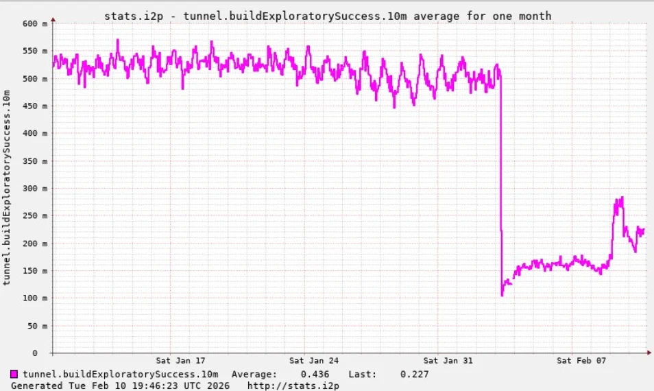
Initial hardware tests of the prototype have yielded impressive results, demonstrating performance improvements of approximately four times compared to comparable 2D chips. Furthermore, the team’s extensive simulations indicate even more substantial gains as the design is scaled up, allowing for additional stacked layers of memory and compute. Projections suggest that with further tiers, the models could achieve up to a twelve-fold improvement on real-world AI workloads, including those derived from Meta’s widely recognized open-source LLaMA model.
Beyond immediate performance enhancements, the researchers also foresee a significant long-term payoff. They posit that this architecture provides a practical pathway to achieve 100 to 1,000-fold improvements in the Energy Delay Product (EDP). EDP is a critical metric that quantifies the combined efficiency of a chip in terms of both speed and energy consumption. By drastically reducing the distances data must travel and introducing a multitude of vertical pathways for data movement, the 3D chip can simultaneously increase throughput and decrease the energy required per operation – a synergistic outcome that has been exceptionally difficult to achieve with traditional flat chip designs.
The significance of this work extends beyond mere performance metrics. By successfully demonstrating the feasibility of producing monolithic 3D chips within the United States, the team asserts that they have laid out a blueprint for a new era of domestic hardware innovation. This era envisions the design and manufacturing of the most advanced chips on U.S. soil, fostering technological sovereignty and economic competitiveness.
Moreover, the paradigm shift towards vertical, monolithic 3D integration will necessitate the cultivation of a new generation of engineers proficient in these advanced methodologies. This echoes the transformative impact of the integrated circuit boom in the 1980s, which was largely propelled by students acquiring expertise in chip design and fabrication within U.S. laboratories. Through strategic collaborations and dedicated funding initiatives, such as the Microelectronics Commons California-Pacific-Northwest AI Hardware Hub (Northwest-AI-Hub), students and researchers are already being actively prepared to drive American semiconductor innovation forward.
H.-S. Philip Wong, the Willard R. and Inez Kerr Bell Professor in the Stanford School of Engineering and a principal investigator of the Northwest-AI-Hub, eloquently summarized the dual imperative: "Breakthroughs like this are of course about performance. But they’re also about capability. If we can build advanced 3D chips, we can innovate faster, respond faster, and shape the future of AI hardware." This sentiment encapsulates the strategic advantage conferred by mastering advanced chip architectures.
The collaborative research efforts were conducted at the Stanford University School of Engineering, Carnegie Mellon University College of Engineering, the University of Pennsylvania School of Engineering and Applied Science, and the Massachusetts Institute of Technology. All fabrication processes were completed at SkyWater Technology’s foundry in Bloomington, Minnesota. The project received crucial support from a diverse range of esteemed organizations, including the Defense Advanced Research Projects Agency, the U.S. National Science Foundation Graduate Research Fellowship Program, Samsung, the Stanford Precourt Institute for Energy, the Stanford SystemX Alliance, the Department of War’s Microelectronics Commons AI Hardware Hub, the U.S. Department of Energy, and the National Science Foundation’s Future of Semiconductors Program (grant number 2425218). Additional contributions to the research came from Stanford co-authors Suhyeong Choi, Samuel Dayo, Andrew Bechdolt, Shengman Li, Dennis T. Rich, and R.H. Yang, as well as other contributing authors from Carnegie Mellon University and MIT.