Unlike the predominantly flat, two-dimensional (2D) chips that characterize most modern computing, this pioneering prototype is engineered to ascend vertically. Imagine a skyscraper where ultra-thin components are meticulously stacked like floors, and vertical wiring acts as a network of high-speed elevators, capable of transporting immense volumes of data with unprecedented rapidity. The design boasts a record-breaking density of vertical connections and a meticulously interwoven layout that strategically places memory and computing units in close proximity. This proximity is crucial, as it effectively circumvents the debilitating slowdowns that have plagued the advancement of flat chip designs. In rigorous hardware tests and extensive simulations, this innovative 3D chip has demonstrated performance improvements that eclipse its 2D counterparts by approximately an order of magnitude.
While academic researchers have previously explored experimental 3D chip designs in laboratory settings, this latest development marks a pivotal moment. It is the first time such a chip has not only delivered demonstrable performance enhancements but has also been successfully produced within a commercial foundry. "This opens the door to a new era of chip production and innovation," declared Subhasish Mitra, the esteemed William E. Ayer Professor in Electrical Engineering and professor of computer science at Stanford University, and the principal investigator behind a new paper detailing this chip, which was presented at the 71st Annual IEEE International Electron Devices Meeting (IEDM). He further emphasized, "Breakthroughs like this are how we get to the 1,000-fold hardware performance improvements future AI systems will demand."
The Achilles’ Heel of Flat Chips in the Age of Modern AI
The insatiable appetite for data processing in large AI models, exemplified by the capabilities of systems like ChatGPT and Claude, necessitates the constant and rapid shuttling of enormous datasets between memory modules, which serve as data repositories, and the computing units responsible for their intricate processing.
On conventional 2D chips, where all components reside on a single plane, memory is inherently limited and spatially dispersed. This physical constraint forces data to traverse a restricted number of long and congested pathways. Consequently, the computing elements, capable of executing operations at remarkable speeds, frequently find themselves idle, waiting for data to arrive. The chip struggles to maintain sufficient memory in close proximity to these processing units, leading to pervasive delays. Engineers refer to this pervasive impediment as the "memory wall," a phenomenon where the processing speed of the chip is outpaced by its ability to deliver the necessary data.
For years, the semiconductor industry has attempted to surmount the memory wall by relentlessly shrinking transistors—the minuscule switches that perform computations and store data—and by increasing their density on each chip. However, researchers contend that this strategy is approaching its fundamental physical limitations, a barrier often termed the "miniaturization wall."
The innovative 3D chip design presented here offers a compelling solution to transcend both these formidable challenges by shifting the paradigm of chip architecture from two dimensions to three. "By integrating memory and computation vertically, we can move a lot more information much quicker, just as the elevator banks in a high-rise let many residents travel between floors at once," explained Tathagata Srimani, assistant professor of electrical and computer engineering at Carnegie Mellon University and the paper’s senior author. Srimani, who initiated this groundbreaking work as a postdoctoral fellow under Mitra’s guidance, eloquently illustrates the efficiency gains.
"The memory wall and the miniaturization wall form a deadly combination," commented Robert M. Radway, assistant professor of electrical and systems engineering at the University of Pennsylvania and a co-author of the study. "We attacked it head-on by tightly integrating memory and logic and then building upward at extremely high density. It’s like the Manhattan of computing — we can fit more people in less space." This analogy powerfully conveys the concept of maximizing efficiency and capacity within a confined footprint.
The Manufacturing Marvel: Crafting the Monolithic 3D Chip
Previous endeavors in 3D chip development often relied on a more straightforward approach: stacking pre-fabricated individual chips. While this method offers some advantages, the interconnections between these stacked layers are typically less refined, limited in number, and can themselves become significant bottlenecks.
This research team, however, has embraced a distinctly more sophisticated methodology. Instead of fabricating separate chips and subsequently bonding them together, they meticulously construct each new layer directly atop the preceding one within a single, unbroken manufacturing flow. This technique, known as "monolithic" 3D integration, employs temperatures sufficiently low to prevent any damage to the circuitry already established in the lower layers. This crucial capability allows for significantly tighter layer stacking and the creation of vastly denser interconnections between them.
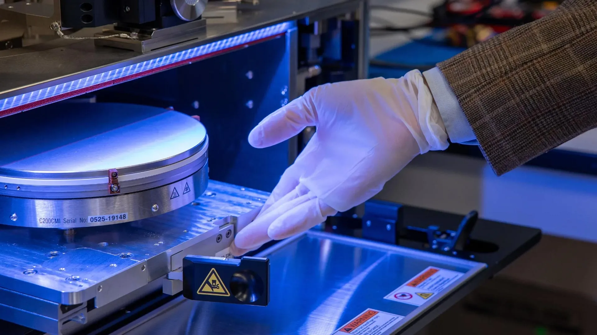
A paramount achievement highlighted by the researchers is that the entire fabrication process was executed within a domestic commercial silicon foundry. "Turning a cutting-edge academic concept into something a commercial fab can build is an enormous challenge," stated co-author Mark Nelson, vice president of technology development operations at SkyWater Technology. He further underscored the strategic importance: "This shows that these advanced architectures aren’t just possible in the lab — they can be produced domestically, at scale, which is what America needs to stay at the forefront of semiconductor innovation." This success story directly addresses national security and economic competitiveness concerns.
Unleashing Performance Gains and Charting the Future of AI Hardware
Initial hardware tests of the prototype have revealed performance improvements of approximately four times compared to comparable 2D chips. The research team’s sophisticated simulations indicate even more substantial gains as the design is scaled upward, incorporating additional stacked layers of memory and compute. Projections suggest that with further tiers, the models could achieve up to a twelvefold improvement on authentic AI workloads, including those derived from Meta’s widely recognized open-source LLaMA model.
Beyond immediate performance boosts, the researchers foresee a more profound long-term benefit. They assert that this architecture provides a viable pathway towards achieving an astonishing 100 to 1,000-fold improvement in the Energy Delay Product (EDP). EDP is a critical metric that judiciously combines computational speed with energy efficiency. By dramatically reducing the distances data must traverse and by introducing a multitude of vertical pathways for data movement, the chip can simultaneously enhance throughput and decrease the energy consumed per operation—a dual objective that has proven exceptionally elusive with conventional flat chip designs.
The significance of this work extends beyond mere speed enhancements. By demonstrating the feasibility of manufacturing monolithic 3D chips within the United States, the researchers posit that this breakthrough offers a blueprint for a new epoch of domestic hardware innovation. This new era will empower the nation to design and manufacture the most advanced chips on U.S. soil, fostering technological sovereignty and economic growth.
Furthermore, the team acknowledges that the transition to vertical, monolithic 3D integration will necessitate the cultivation of a new generation of engineers proficient in these advanced methodologies. This parallels the transformative impact of the integrated circuit revolution in the 1980s, which was significantly propelled by students acquiring expertise in chip design and fabrication within U.S. laboratories. Through proactive collaborations and strategic funding initiatives, such as those supported by the Microelectronics Commons California-Pacific-Northwest AI Hardware Hub (Northwest-AI-Hub), students and researchers are already being actively prepared to propel American semiconductor innovation into the future.
"Breakthroughs like this are of course about performance," affirmed H.-S. Philip Wong, the Willard R. and Inez Kerr Bell Professor in the Stanford School of Engineering and principal investigator of the Northwest-AI-Hub. "But they’re also about capability. If we can build advanced 3D chips, we can innovate faster, respond faster, and shape the future of AI hardware." This sentiment encapsulates the multifaceted impact of this groundbreaking achievement.
The research leading to this pivotal advancement was conducted across the Stanford University School of Engineering, Carnegie Mellon University College of Engineering, the University of Pennsylvania School of Engineering and Applied Science, and the Massachusetts Institute of Technology. All fabrication processes were meticulously completed at SkyWater Technology’s Bloomington, Minnesota, Foundry. Crucial support for this endeavor was provided by a consortium of esteemed organizations, including the Defense Advanced Research Projects Agency, the U.S. National Science Foundation Graduate Research Fellowship Program, Samsung, the Stanford Precourt Institute for Energy, the Stanford SystemX Alliance, the Department of War’s Microelectronics Commons AI Hardware Hub, the U.S. Department of Energy, and the National Science Foundation’s Future of Semiconductors Program (grant number 2425218). Additional Stanford co-authors contributing to this seminal study include Suhyeong Choi, Samuel Dayo, Andrew Bechdolt, Shengman Li, Dennis T. Rich, and R.H. Yang. Further contributions were made by researchers from Carnegie Mellon University and MIT.