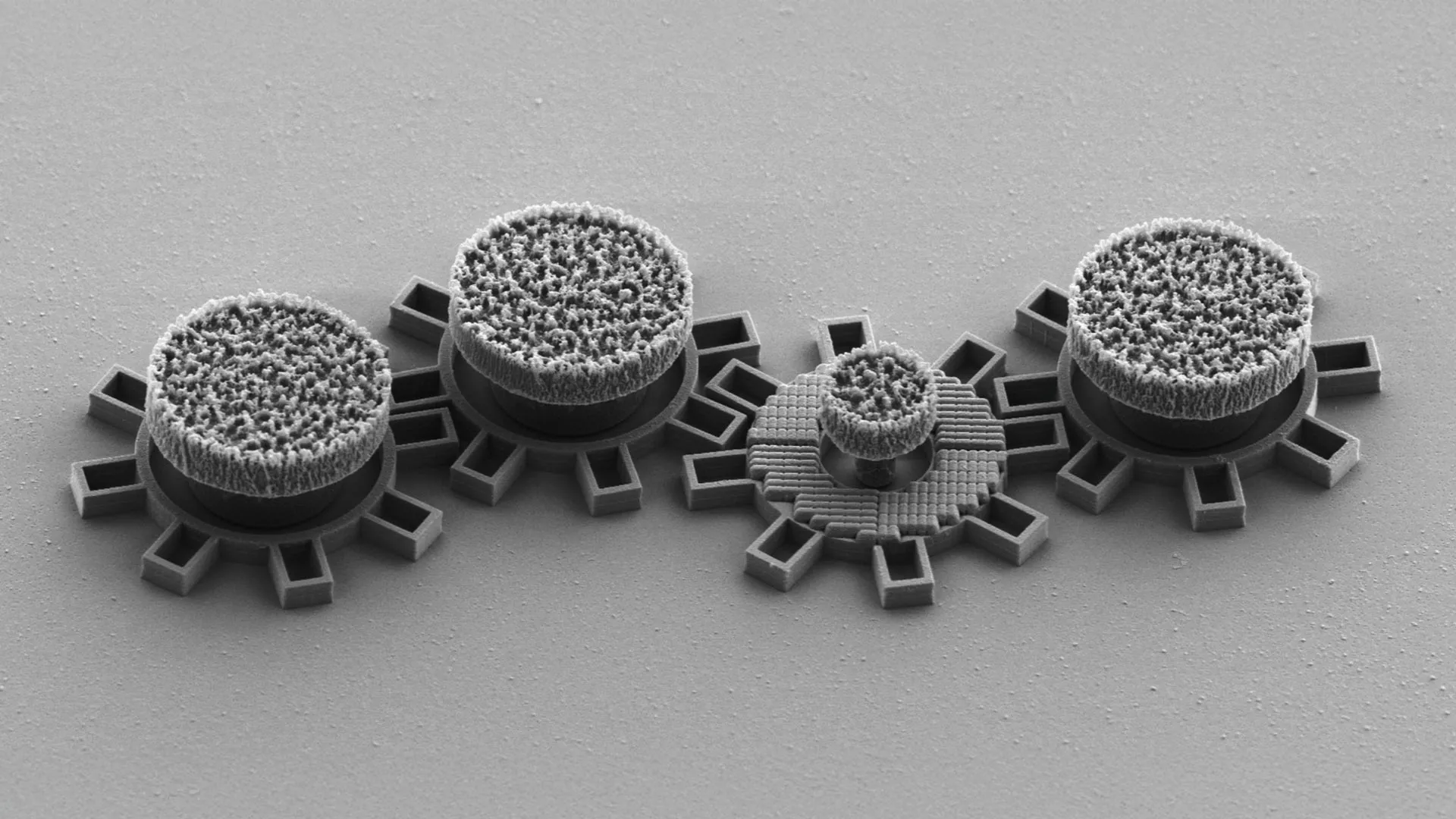
Unlike the predominantly flat, two-dimensional (2D) chips that define today’s computing landscape, this novel prototype is engineered for vertical expansion, resembling the layered structure of a skyscraper. Ultra-thin components are stacked like floors, interconnected by an intricate network of vertical wiring that functions as a high-speed elevator system, enabling the rapid and efficient movement of vast quantities of data. The chip boasts a record-setting number of vertical connections and a densely interwoven design that strategically places memory and computing units in close proximity. This proximity is crucial for overcoming the inherent slowdowns that have historically constrained the performance of flat chips. In rigorous hardware tests and extensive simulations, this 3D chip has demonstrated a remarkable performance advantage, outperforming its 2D counterparts by approximately an order of magnitude.
While experimental 3D chips have been developed in academic settings previously, this represents the first instance where a 3D chip has not only delivered tangible performance enhancements but has also been produced within a commercial foundry. "This opens the door to a new era of chip production and innovation," stated Subhasish Mitra, the William E. Ayer Professor in Electrical Engineering and professor of computer science at Stanford University, and the principal investigator of a seminal paper detailing this advancement, presented at the 71st Annual IEEE International Electron Devices Meeting (IEDM). He further emphasized, "Breakthroughs like this are how we get to the 1,000-fold hardware performance improvements future AI systems will demand."
The Pervasive Challenge of the "Memory Wall" in Modern AI
The insatiable appetite for data processing in large-scale AI models, such as those powering applications like ChatGPT and Claude, necessitates constant, high-volume data shuttling between memory units, which store information, and the computing units responsible for its processing. In conventional 2D chips, where all components reside on a single surface, memory is inherently limited and often dispersed. This spatial separation forces data to traverse lengthy, congested pathways, creating a significant bottleneck. The computing units, capable of processing information at remarkable speeds, frequently find themselves waiting for data to arrive, a phenomenon engineers term the "memory wall." This limitation stems from the chip’s inability to keep sufficient memory in close proximity to the processing elements.
For years, the semiconductor industry has attempted to push back against this memory wall by relentlessly shrinking transistors—the fundamental building blocks of computation and data storage—and increasing their density on each chip. However, researchers now acknowledge that this approach is approaching its absolute physical limits, a constraint commonly referred to as the "miniaturization wall."
The newly developed 3D chip architecture directly confronts and aims to surmount both of these formidable barriers by embracing verticality. "By integrating memory and computation vertically, we can move a lot more information much quicker, just as the elevator banks in a high-rise let many residents travel between floors at once," explained Tathagata Srimani, assistant professor of electrical and computer engineering at Carnegie Mellon University and the paper’s senior author, who initiated this research as a postdoctoral fellow under Mitra’s guidance.
Robert M. Radway, assistant professor of electrical and systems engineering at the University of Pennsylvania and a co-author of the study, articulated the gravity of the situation: "The memory wall and the miniaturization wall form a deadly combination. We attacked it head-on by tightly integrating memory and logic and then building upward at extremely high density. It’s like the Manhattan of computing — we can fit more people in less space."
The Monolithic 3D Chip: A Novel Manufacturing Paradigm
Many prior endeavors in 3D chip development have adopted a more straightforward approach, involving the stacking of pre-fabricated, separate chips. While this method offers some advantages, the inter-layer connections tend to be relatively rudimentary, limited in number, and often become points of performance constriction.
This research team, however, has pioneered a distinct manufacturing strategy. Instead of producing individual chips and subsequently bonding them, they meticulously build each new layer directly atop the preceding one in a single, continuous fabrication flow. This technique, known as "monolithic" 3D integration, utilizes processing temperatures that are sufficiently low to prevent any damage to the circuitry already established in the lower layers. This crucial innovation enables the layers to be packed more densely and facilitates the creation of a far greater number of highly efficient connections between them.
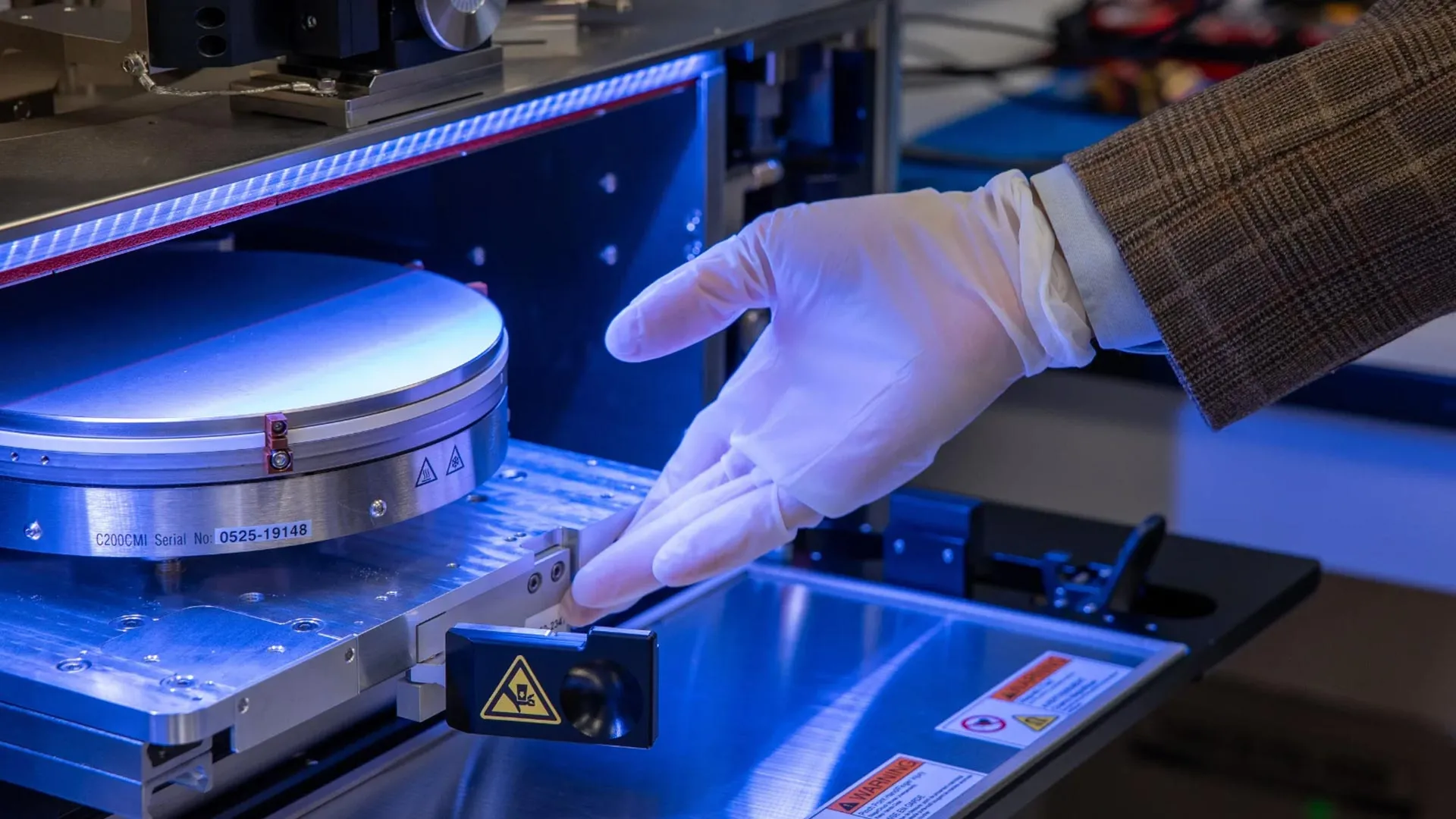
A pivotal aspect highlighted by the researchers is that the entire manufacturing process was successfully executed within a domestic, commercial silicon foundry. "Turning a cutting-edge academic concept into something a commercial fab can build is an enormous challenge," commented co-author Mark Nelson, vice president of technology development operations at SkyWater Technology. He further emphasized the significance of this achievement: "This shows that these advanced architectures aren’t just possible in the lab — they can be produced domestically, at scale, which is what America needs to stay at the forefront of semiconductor innovation."
Quantifiable Performance Gains and the Future Trajectory of AI Hardware
Initial hardware testing has revealed that the prototype chip outperforms comparable 2D chips by approximately fourfold. The team’s sophisticated simulations project even more substantial performance improvements as the design scales vertically, incorporating additional stacked layers of memory and compute. With further tiers of integration, these simulations indicate potential performance gains of up to twelvefold for real-world AI workloads, including those derived from Meta’s open-source LLaMA model.
Beyond immediate performance boosts, the researchers foresee a more profound long-term impact. They assert that this architecture provides a viable pathway toward achieving 100-fold to 1,000-fold improvements in the energy-delay product (EDP)—a critical metric that quantifies the combined efficiency of speed and energy consumption. By drastically reducing the distances data must travel and establishing a multitude of vertical pathways for data movement, the chip can achieve higher throughput while simultaneously lowering the energy expenditure per operation, a synergy that has eluded conventional flat chip designs.
The significance of this breakthrough extends beyond mere computational speed. By demonstrating the feasibility of manufacturing monolithic 3D chips within the United States, the team has laid the groundwork for a new era of domestic hardware innovation, where cutting-edge chip design and fabrication can be conducted entirely on U.S. soil.
Furthermore, the researchers posit that the transition to vertical, monolithic 3D integration will necessitate the cultivation of a new generation of engineers proficient in these advanced methodologies, drawing a parallel to the integrated circuit revolution of the 1980s, which was propelled by students trained in chip design and fabrication within U.S. laboratories. Through ongoing collaborations and strategic funding initiatives, such as the Microelectronics Commons California-Pacific-Northwest AI Hardware Hub (Northwest-AI-Hub), students and researchers are actively being prepared to drive forward American semiconductor innovation.
"Breakthroughs like this are of course about performance," stated H.-S. Philip Wong, the Willard R. and Inez Kerr Bell Professor in the Stanford School of Engineering and principal investigator of the Northwest-AI-Hub. He elaborated, "But they’re also about capability. If we can build advanced 3D chips, we can innovate faster, respond faster, and shape the future of AI hardware."
This pioneering study was a collaborative effort involving researchers from the Stanford University School of Engineering, Carnegie Mellon University College of Engineering, the University of Pennsylvania School of Engineering and Applied Science, and the Massachusetts Institute of Technology. All fabrication processes were meticulously carried out at SkyWater Technology’s Foundry in Bloomington, Minnesota. The project received vital support from a diverse range of esteemed organizations, including the Defense Advanced Research Projects Agency, the U.S. National Science Foundation Graduate Research Fellowship Program, Samsung, the Stanford Precourt Institute for Energy, the Stanford SystemX Alliance, the Department of War’s Microelectronics Commons AI Hardware Hub, the U.S. Department of Energy, and the National Science Foundation’s Future of Semiconductors Program (grant number 2425218).
Additional contributing Stanford co-authors to this groundbreaking work include Suhyeong Choi, Samuel Dayo, Andrew Bechdolt, Shengman Li, Dennis T. Rich, and R.H. Yang. Further research contributions were made by authors from Carnegie Mellon University and MIT.