Unlike the predominantly flat, two-dimensional (2D) chips that dominate the current technological landscape, this innovative prototype is designed with verticality in mind. Imagine a skyscraper where ultra-thin components are stacked like floors, and data, akin to countless residents, is transported with remarkable speed and efficiency via vertical wiring that functions as express elevators. This intricate design boasts a record-breaking number of vertical connections and a meticulously interwoven layout that strategically positions memory and computing units in close proximity. This proximity is crucial as it effectively bypasses the data transfer slowdowns that have historically plagued flat chip architectures. Early hardware tests and extensive simulations have demonstrated that this 3D chip significantly outperforms its 2D counterparts, achieving improvements of approximately an order of magnitude.
While experimental 3D chips have been developed in academic settings before, this marks the first instance where a 3D chip has not only demonstrated clear performance enhancements but has also been successfully manufactured in a commercial foundry. "This opens the door to a new era of chip production and innovation," stated Subhasish Mitra, the William E. Ayer Professor in Electrical Engineering and professor of computer science at Stanford University, and the principal investigator of the seminal paper detailing this chip, which was unveiled at the 71st Annual IEEE International Electron Devices Meeting (IEDM). He further emphasized, "Breakthroughs like this are how we get to the 1,000-fold hardware performance improvements future AI systems will demand."
The Achilles’ Heel of Flat Chips in Modern AI
The insatiable appetite of contemporary AI models, such as ChatGPT and Claude, for data presents a formidable challenge for existing hardware. These sophisticated models continuously shuttle vast quantities of information between memory, which serves as the repository of knowledge, and the computing units responsible for processing it.
On conventional 2D chips, the inherent limitation is that all components reside on a single plane. This often results in memory being dispersed and relatively scarce, forcing data to traverse long, congested pathways. Consequently, the computing elements, capable of processing information at blistering speeds, often find themselves waiting for data to arrive. This bottleneck, colloquially known as the "memory wall," occurs when processing speed outpaces the chip’s capacity to deliver the necessary data.
For years, the semiconductor industry attempted to circumvent the memory wall by relentlessly shrinking transistors—the fundamental building blocks of computation and data storage—and cramming more of them onto each chip. However, researchers contend that this approach is rapidly approaching its physical limitations, a phenomenon referred to as the "miniaturization wall."
The novel 3D chip design directly confronts both of these formidable barriers by embracing verticality. "By integrating memory and computation vertically, we can move a lot more information much quicker, just as the elevator banks in a high-rise let many residents travel between floors at once," explained Tathagata Srimani, assistant professor of electrical and computer engineering at Carnegie Mellon University and the paper’s senior author. Srimani initiated this research as a postdoctoral fellow under Mitra’s guidance.
Robert M. Radway, assistant professor of electrical and systems engineering at the University of Pennsylvania and a co-author of the study, articulated the severity of the problem: "The memory wall and the miniaturization wall form a deadly combination. We attacked it head-on by tightly integrating memory and logic and then building upward at extremely high density. It’s like the Manhattan of computing — we can fit more people in less space."
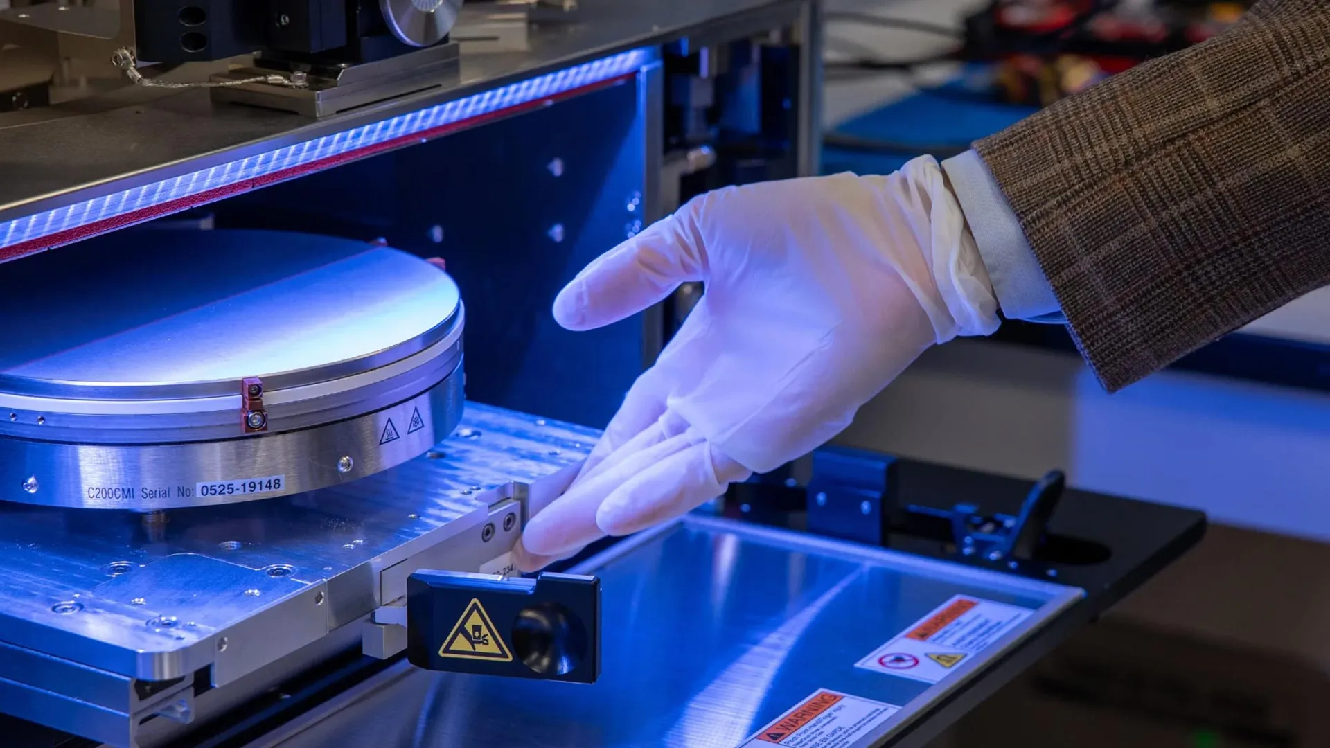
The Manufacturing Process of the Monolithic 3D Chip
Previous attempts at creating 3D chips often involved a more straightforward approach of stacking pre-manufactured chips. While this can offer some advantages, the interconnections between these stacked layers are typically less robust, limited in number, and can easily become points of congestion.
This research team, however, adopted a fundamentally different and more sophisticated methodology. Instead of fabricating separate chips and then bonding them together, they construct each subsequent layer directly atop the preceding one in a continuous, integrated manufacturing flow. This technique, known as "monolithic" 3D integration, operates at temperatures low enough to prevent damage to the circuitry already established in lower layers. This crucial aspect enables the layers to be packed more densely and facilitates the creation of a significantly higher number of connections between them.
A pivotal element of this development, as highlighted by the researchers, is that the entire manufacturing process was executed within a domestic commercial silicon foundry. "Turning a cutting-edge academic concept into something a commercial fab can build is an enormous challenge," commented co-author Mark Nelson, vice president of technology development operations at SkyWater Technology. "This shows that these advanced architectures aren’t just possible in the lab — they can be produced domestically, at scale, which is what America needs to stay at the forefront of semiconductor innovation."
Performance Gains and the Future Trajectory of AI Hardware
Initial hardware testing has revealed that the prototype chip outperforms comparable 2D chips by approximately fourfold. Furthermore, the team’s sophisticated simulations project even more substantial performance gains as the design is scaled up with additional stacked layers of memory and compute. With further tiers, these models predict improvements of up to twelvefold for real-world AI workloads, including those derived from Meta’s open-source LLaMA model.
Beyond immediate performance enhancements, the researchers also foresee a significant long-term benefit. They assert that this architecture provides a practical pathway to achieving 100- to 1,000-fold improvements in the energy delay product (EDP)—a critical metric that quantifies the combined efficiency of speed and power consumption. By dramatically reducing the distances data must travel and introducing a multitude of vertical pathways, the chip can simultaneously boost throughput and lower the energy required per operation, a feat that has proven exceptionally challenging with conventional flat designs.
The significance of this work extends beyond mere performance metrics. By demonstrating the feasibility of manufacturing monolithic 3D chips within the United States, the team offers a compelling blueprint for a new era of domestic hardware innovation. This advancement promises to enable the design and production of the most advanced chips on American soil, fostering greater technological independence and leadership.
Moreover, the transition to vertical, monolithic 3D integration necessitates the cultivation of a new generation of engineers proficient in these advanced methodologies. This mirrors the transformative impact of the integrated circuit revolution in the 1980s, which was propelled by students acquiring chip design and fabrication expertise in U.S. laboratories. Through collaborative initiatives and strategic funding, such as the Microelectronics Commons California-Pacific-Northwest AI Hardware Hub (Northwest-AI-Hub), educational programs are already in place to equip students and researchers for the challenges and opportunities ahead, thereby driving American semiconductor innovation forward.
"Breakthroughs like this are of course about performance," observed H.-S. Philip Wong, the Willard R. and Inez Kerr Bell Professor in the Stanford School of Engineering and principal investigator of the Northwest-AI-Hub. "But they’re also about capability. If we can build advanced 3D chips, we can innovate faster, respond faster, and shape the future of AI hardware."
This pioneering study was a collaborative effort involving the Stanford University School of Engineering, the Carnegie Mellon University College of Engineering, the University of Pennsylvania School of Engineering and Applied Science, and the Massachusetts Institute of Technology. All fabrication processes were meticulously executed at SkyWater Technology’s Bloomington, Minnesota, Foundry. The research received crucial support from a diverse range of organizations, including the Defense Advanced Research Projects Agency, the U.S. National Science Foundation Graduate Research Fellowship Program, Samsung, the Stanford Precourt Institute for Energy, the Stanford SystemX Alliance, the Department of War’s Microelectronics Commons AI Hardware Hub, the U.S. Department of Energy, and the National Science Foundation’s Future of Semiconductors Program (grant number 2425218). Additional Stanford co-authors contributing to this groundbreaking work include Suhyeong Choi, Samuel Dayo, Andrew Bechdolt, Shengman Li, Dennis T. Rich, and R.H. Yang. Further contributions were made by researchers from Carnegie Mellon University and MIT.