Engineers from a formidable consortium of leading academic institutions – Stanford University, Carnegie Mellon University, the University of Pennsylvania, and the Massachusetts Institute of Technology – have joined forces with SkyWater Technology, the nation’s largest exclusively U.S.-based pure-play semiconductor foundry, to engineer a revolutionary multilayer computer chip. This novel architecture, the team asserts, is poised to precipitate a seismic shift in the realm of artificial intelligence hardware and significantly bolster domestic semiconductor innovation, addressing critical limitations that have long hampered the advancement of AI.
Unlike the vast majority of contemporary chips, which are predominantly flat and two-dimensional, this pioneering prototype is meticulously designed to ascend vertically, mimicking the layered structure of a skyscraper. Ultra-thin components are ingeniously stacked like floors, while an intricate network of vertical wiring functions as a fleet of high-speed elevators, facilitating the rapid transit of immense volumes of data. This sophisticated design boasts a record-shattering number of vertical connections and an exceptionally dense, interwoven layout that strategically positions memory and computing units in close proximity. This proximity is crucial, as it effectively circumvents the performance degradation that has plagued conventional flat chip designs. In rigorous hardware tests and extensive simulations, the 3D chip has demonstrated a remarkable performance improvement, outperforming its 2D counterparts by an order of magnitude, a feat that signifies a monumental leap forward.
While experimental 3D chips have been conceptualized and constructed in academic laboratories previously, this development marks the first instance where a 3D chip has delivered demonstrably clear performance enhancements and, crucially, has been successfully manufactured within a commercial foundry. Subhasish Mitra, the William E. Ayer Professor in Electrical Engineering and a professor of computer science at Stanford University, and the principal investigator of a seminal paper detailing this breakthrough presented at the 71st Annual IEEE International Electron Devices Meeting (IEDM), expressed profound optimism. "This opens the door to a new era of chip production and innovation," Mitra declared. "Breakthroughs like this are how we get to the 1,000-fold hardware performance improvements future AI systems will demand." This sentiment underscores the transformative potential of this innovation for the future of artificial intelligence.
The Inherent Limitations of Flat Chips in the Face of Modern AI Demands
The escalating complexity and sheer scale of modern AI models, exemplified by behemoths like ChatGPT and Claude, necessitate the constant and rapid shuttling of enormous datasets between memory units, which store the vital information, and the processing units responsible for its analysis. This relentless data movement represents a significant bottleneck.
On conventional 2D chips, where all components reside on a single planar surface, memory capacity is often constrained and geographically dispersed. This spatial limitation forces data to traverse lengthy, congested pathways, creating a bottleneck. The processing units within these chips possess the capability to operate at speeds far exceeding the rate at which data can be delivered from memory. Furthermore, the chip struggles to maintain an adequate supply of nearby memory. The inevitable consequence of this disparity is frequent and costly idle time, wherein the processing units are forced to wait for data. Engineers have aptly termed this pervasive issue the "memory wall," a formidable barrier where processing speed outstrips the chip’s capacity to supply the necessary data.
For years, the semiconductor industry has grappled with the memory wall by relentlessly pursuing the miniaturization of transistors – the microscopic switches that execute computations and store data – and by increasing their density on each chip. However, researchers now contend that this approach is approaching fundamental physical limitations, a concept they refer to as the "miniaturization wall."
The innovative new 3D chip design endeavors to surmount both of these critical limitations by embracing a vertical construction paradigm. Tathagata Srimani, an assistant professor of electrical and computer engineering at Carnegie Mellon University and the paper’s senior author, who initiated this research as a postdoctoral fellow under Mitra’s guidance, drew an insightful analogy. "By integrating memory and computation vertically, we can move a lot more information much quicker, just as the elevator banks in a high-rise let many residents travel between floors at once," Srimani explained. This analogy effectively captures the essence of how vertical integration facilitates massively parallel data transfer.
Robert M. Radway, an assistant professor of electrical and systems engineering at the University of Pennsylvania and a co-author of the study, emphasized the synergistic nature of these challenges. "The memory wall and the miniaturization wall form a deadly combination," Radway stated. "We attacked it head-on by tightly integrating memory and logic and then building upward at extremely high density. It’s like the Manhattan of computing – we can fit more people in less space." This powerful metaphor highlights the efficiency and density achieved through the novel architectural approach.
The Manufacturing Process of the Monolithic 3D Chip: A Paradigm Shift
Many prior attempts at developing 3D chips have adopted a more rudimentary approach, involving the stacking of pre-fabricated, separate chips. While this method can offer some advantages, the interconnections between these stacked layers often prove to be relatively rudimentary, limited in number, and can consequently become significant performance bottlenecks.
This pioneering team, however, has implemented a fundamentally different and more sophisticated methodology. Rather than fabricating individual chips and subsequently bonding them together, they meticulously construct each successive layer directly atop the preceding one in a continuous, uninterrupted manufacturing flow. This process, known as "monolithic" 3D integration, operates at temperatures sufficiently low to prevent any damage to the circuitry already established in the lower layers. This crucial capability allows for significantly tighter stacking of layers and the creation of a far greater density of interconnections between them, unlocking unprecedented levels of integration.
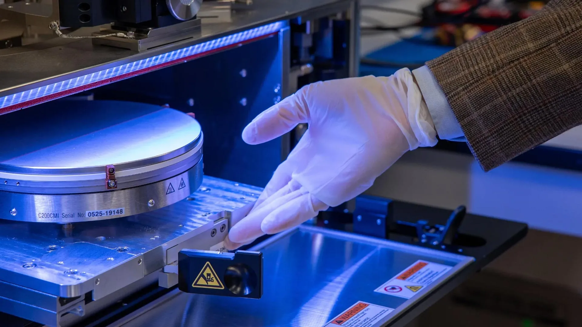
A particularly significant aspect of this achievement, according to the researchers, is that the entire manufacturing process was successfully executed within a domestic, commercial silicon foundry. Mark Nelson, vice president of technology development operations at SkyWater Technology and a co-author, underscored the magnitude of this accomplishment. "Turning a cutting-edge academic concept into something a commercial fab can build is an enormous challenge," Nelson remarked. "This shows that these advanced architectures aren’t just possible in the lab – they can be produced domestically, at scale, which is what America needs to stay at the forefront of semiconductor innovation." This statement firmly positions the project as a vital step towards re-establishing U.S. leadership in semiconductor manufacturing.
Demonstrable Performance Gains and the Future Trajectory of AI Hardware
In initial hardware evaluations, the prototype chip exhibited a performance increase of approximately fourfold when compared to comparable 2D chips. The team’s extensive simulations indicate even more substantial performance gains as the design evolves to incorporate additional stacked layers of memory and compute. Projections suggest that with further tiers, the models could achieve up to a twelvefold improvement on real-world AI workloads, including those derived from Meta’s widely adopted open-source LLaMA model. This level of performance enhancement is transformative for the practical application of AI.
Beyond immediate performance metrics, the researchers also highlight a long-term, significant benefit. They assert that this architecture provides a practical and achievable pathway to achieving 100 to 1,000-fold improvements in the energy delay product (EDP). EDP is a critical metric that quantifies both the speed of computation and its energy efficiency. By drastically reducing the distances data must travel and by providing a multitude of vertical pathways for data movement, the chip can simultaneously boost throughput and decrease the energy consumed per operation – a combination that has historically been exceedingly difficult to attain with conventional flat chip designs.
The significance of this research extends beyond mere speed enhancements. By demonstrating the feasibility of producing monolithic 3D chips within the United States, the team argues that this work provides a clear blueprint for a new era of domestic hardware innovation. This new era promises the capability to design and manufacture the most advanced chips on U.S. soil, bolstering national technological sovereignty and economic competitiveness.
Furthermore, the researchers posit that the transition to vertical, monolithic 3D integration will necessitate the cultivation of a new generation of engineers proficient in these advanced methodologies. This paradigm shift is anticipated to mirror the revolutionary impact of the integrated circuit boom in the 1980s, which was largely fueled by students acquiring expertise in chip design and fabrication within U.S. laboratories. Through robust collaborations and strategic funding initiatives, such as those supported by the Microelectronics Commons California-Pacific-Northwest AI Hardware Hub (Northwest-AI-Hub), students and researchers are already actively being prepared to drive American semiconductor innovation forward.
H.-S. Philip Wong, the Willard R. and Inez Kerr Bell Professor in the Stanford School of Engineering and a principal investigator of the Northwest-AI-Hub, eloquently summarized the broader implications. "Breakthroughs like this are of course about performance," Wong stated. "But they’re also about capability. If we can build advanced 3D chips, we can innovate faster, respond faster, and shape the future of AI hardware." This profound statement encapsulates the multifaceted advantages offered by this technological leap.
The collaborative research effort spanned multiple prestigious institutions, including the Stanford University School of Engineering, the Carnegie Mellon University College of Engineering, the University of Pennsylvania School of Engineering and Applied Science, and the Massachusetts Institute of Technology. All fabrication processes were expertly completed at SkyWater Technology’s Bloomington, Minnesota, Foundry. The project received crucial support from a diverse array of esteemed organizations, including the Defense Advanced Research Projects Agency, the U.S. National Science Foundation Graduate Research Fellowship Program, Samsung, the Stanford Precourt Institute for Energy, the Stanford SystemX Alliance, the Department of War’s Microelectronics Commons AI Hardware Hub, the U.S. Department of Energy, and the National Science Foundation’s Future of Semiconductors Program (grant number 2425218). Additional contributions from Stanford University include co-authors Suhyeong Choi, Samuel Dayo, Andrew Bechdolt, Shengman Li, Dennis T. Rich, and R.H. Yang. Further contributions were made by researchers from Carnegie Mellon University and the Massachusetts Institute of Technology, solidifying this as a truly collaborative and impactful endeavor.