

 Imroatul Nasiyah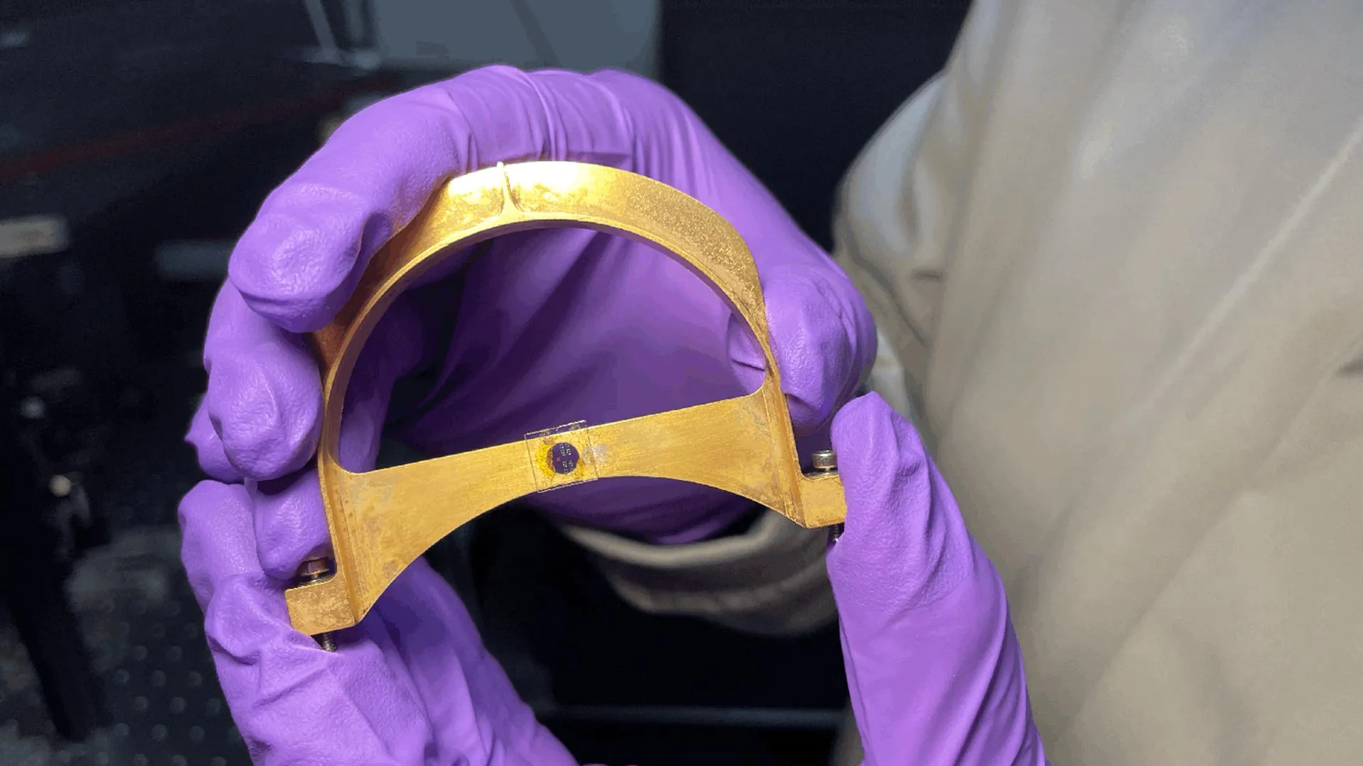
The core of this advancement lies in the device’s ability to foster entanglement, a fundamental quantum phenomenon where particles become interconnected in such a way that they share the same fate, regardless of the distance separating them. This entanglement between photons, the fundamental particles of light, and electrons, the charge carriers crucial for computation, is considered an indispensable prerequisite for the realization of robust quantum communication networks. "The material in question is not really new, but the way we use it is," explained Jennifer Dionne, a distinguished professor of materials science and engineering at Stanford and the senior author of the study. "It provides a very versatile, stable spin connection between electrons and photons that is the theoretical basis of quantum communication. Typically, however, the electrons lose their spin too quickly to be useful." This inherent instability of electron spin at ambient temperatures has been a major hurdle, and the Stanford team’s innovation directly addresses this challenge.
The novel device ingeniously combines a meticulously patterned thin layer of molybdenum diselenide (MoSe2) with a specially engineered nanopatterned silicon substrate. Molybdenum diselenide belongs to a class of materials known as transition metal dichalcogenides (TMDCs), which have garnered significant attention for their exceptional optical and quantum properties. These materials exhibit unique electronic band structures and strong light-matter interactions, making them ideal candidates for quantum applications. The researchers highlighted that the silicon nanostructures are not merely passive components but actively contribute to the functionality of the device by generating what they term "twisted light."
"The Silicon nanostructures enable what we call ‘twisted light,’" elaborated Feng Pan, a postdoctoral scholar in Dionne’s lab and the paper’s first author. "The photons spin in a corkscrew fashion, but more importantly, we can use these spinning photons to impart spin on electrons that are the heart of quantum computing." This concept of "twisted light," also known as orbital angular momentum (OAM) of light, refers to photons that carry an additional degree of freedom beyond their polarization. This OAM can be manipulated and transferred to other quantum systems, such as electron spins. The Stanford team’s design precisely controls the OAM of photons by shaping the light’s wavefront through the silicon nanostructures, creating a highly localized and intense light field.
Dionne further emphasized the microscopic scale of these intricate structures, noting their size is comparable to the wavelengths of visible light, rendering them invisible to the naked eye. "The patterned nanostructures are imperceptible to the human eye, about the size of the wavelength of visible light," Dionne stated. "But they help us manipulate photons very precisely to make them spin — to twist them- in a specific direction, for example, up or down." This precise control over photon spin is paramount for encoding quantum information.
The ability to harness this twisted light opens a direct pathway to entangling it with electron spins, thereby creating qubits. Qubits, the fundamental units of quantum information, are the building blocks of quantum computers and quantum communication systems. Unlike classical bits that can only represent a 0 or a 1, qubits can exist in a superposition of both states simultaneously, a quantum mechanical principle that allows for exponentially more powerful computation and communication capabilities. The stability of these quantum states is crucial, and conventional quantum systems often require extreme cooling to combat decoherence, the loss of quantum information due to environmental interactions.
The Stanford device’s operation at room temperature bypasses this significant obstacle, eliminating the need for expensive and cumbersome cooling infrastructure. This makes quantum technologies more practical and economically viable for a wider range of applications. The researchers also pointed out the compact and relatively inexpensive nature of their design when compared to existing quantum systems, which are often large, complex, and prohibitively expensive. If further developed and scaled, this technology holds the potential to drive advancements in numerous fields, including secure communication networks that are impervious to eavesdropping, highly sensitive sensors for scientific research and medical diagnostics, and accelerated progress in high-performance computing and artificial intelligence.
The selection of TMDC materials was deliberate, driven by their intrinsic quantum characteristics that facilitate strong light-matter interactions. The research team collaborated with Stanford experts Fang Liu and Tony Heinz, who possess specialized knowledge in these materials, to optimize the MoSe2 layer for enhanced quantum performance. "It all comes down to this material and our Silicon chip," Pan affirmed. "Together, they efficiently confine and enhance the twisting of light to create a strong coupling of spin between photons and electrons. This stabilizes the quantum state that makes quantum communication possible." This synergistic interplay between the TMDC and the silicon nanostructures significantly amplifies the interaction strength, thereby preserving the delicate quantum states necessary for reliable information processing and transmission.
Looking ahead, the researchers are actively engaged in refining their device and exploring other TMDC materials and combinations that could offer even superior performance. They are also investigating the possibility that these room-temperature systems might unlock novel quantum capabilities that are currently only observable under extreme conditions. A long-term aspiration is the integration of these miniaturized quantum components into larger, interconnected quantum networks. Realizing this ambitious vision will necessitate further advancements in supporting technologies, including more efficient light sources, sophisticated modulators and detectors, and robust interconnects for seamless data transfer.
Ultimately, the overarching goal is to miniaturize quantum components to such an extent that they can be integrated into everyday electronic devices. While this future may still be many years away, the current work represents a pivotal step toward democratizing quantum technology and making it more accessible and practical for widespread adoption. "If we can do that, maybe someday we could do quantum computing in a cell phone," Pan mused with a smile, acknowledging the long-term trajectory of this research, which he estimates to be at least a decade away from such transformative consumer applications. This Stanford breakthrough, by cleverly manipulating light at the nanoscale and enabling quantum phenomena at room temperature, has laid a crucial foundation for the next generation of quantum technologies, promising to redefine the boundaries of computation and communication.