The core innovation of this remarkable chip lies in its design, which is specifically engineered to perform convolution operations. These operations are not merely a secondary function but rather a fundamental and indispensable component of machine learning algorithms. Their crucial role enables AI systems to meticulously identify and interpret intricate patterns within vast datasets, including images, video streams, and textual information. Conventionally, these convolution operations demand substantial computational resources and, consequently, a significant amount of electrical energy. The University of Florida researchers have ingeniously overcome this limitation by integrating optical components directly onto a silicon chip. This elegant integration creates a synergistic system that executes convolutions using precisely controlled laser light and an array of microscopic lenses. The result is a dramatic reduction in energy consumption, often by orders of magnitude, and a significant acceleration of processing speeds, ushering in a new paradigm for AI computation.
The transformative potential of this development is underscored by the enthusiastic remarks of the study’s leader, Volker J. Sorger, who holds the esteemed position of Rhines Endowed Professor in Semiconductor Photonics at the University of Florida. "Performing a key machine learning computation at near zero energy is a leap forward for future AI systems," Professor Sorger stated, emphasizing the monumental significance of their achievement. He further elaborated on the critical importance of this breakthrough for the continued advancement and scalability of AI capabilities in the years to come, highlighting its role in enabling the next generation of intelligent systems.
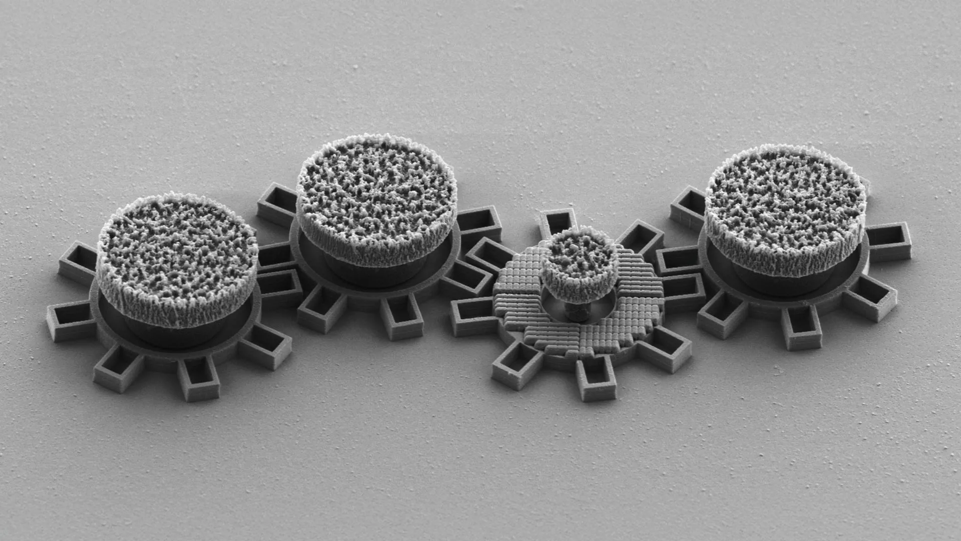
In rigorous testing, the prototype chip has demonstrated exceptional performance. It successfully classified handwritten digits with an accuracy rate of approximately 98 percent, a level of precision that is directly comparable to that achieved by conventional, purely electronic chips. The underlying mechanism of this optical computation involves two sets of miniature Fresnel lenses. These lenses, which are flat and remarkably ultrathin versions of the larger, more familiar lenses found in lighthouses, are meticulously fabricated using established and widely adopted semiconductor manufacturing techniques. The precision of this fabrication is astounding, with these lenses measuring narrower than a human hair and being directly etched onto the surface of the chip, showcasing the team’s mastery of nanoscale engineering.
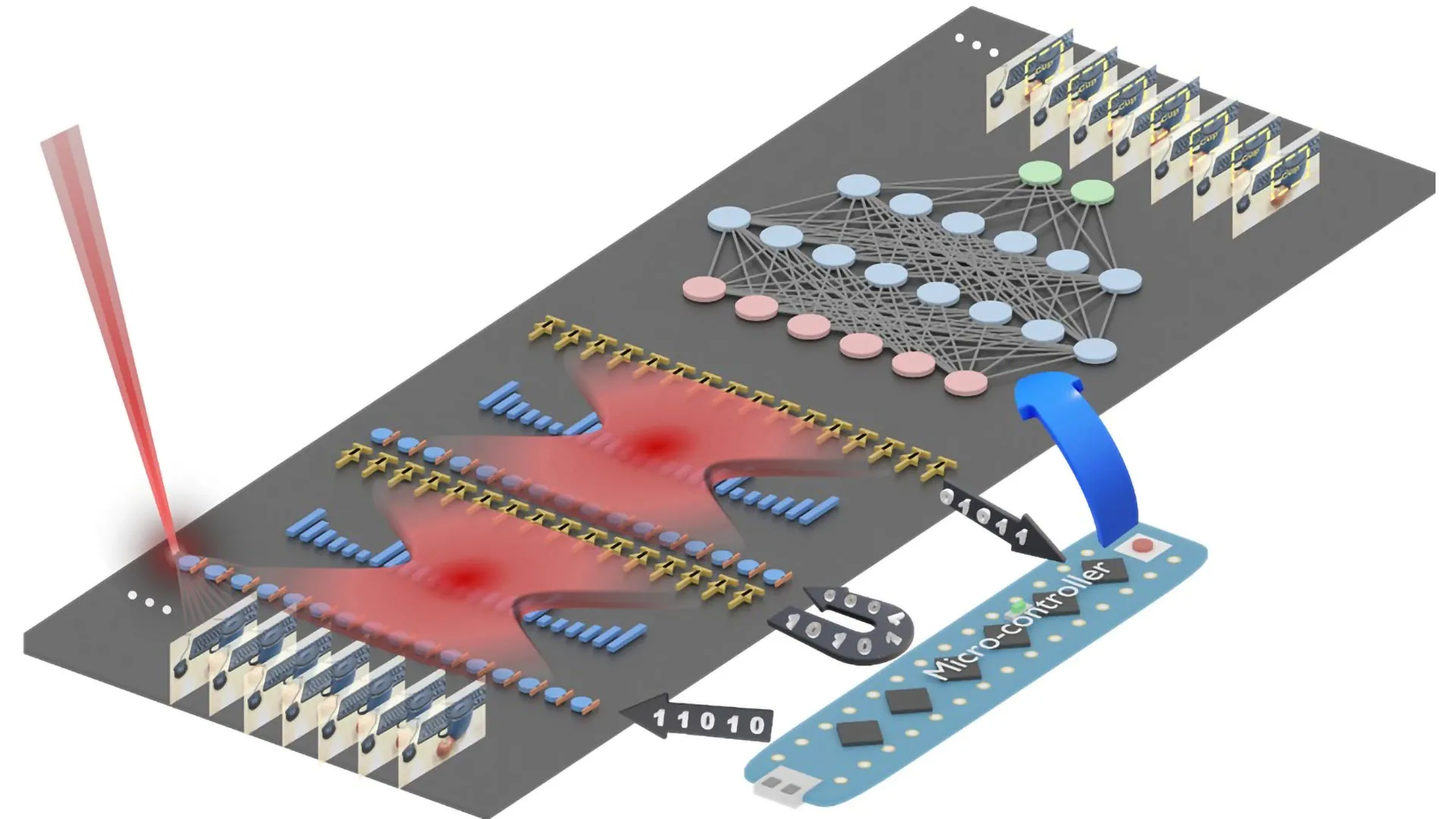
The process by which the chip performs a convolution is a sophisticated interplay of light and computation. Initially, the machine learning data, which is inherently digital, is meticulously converted into laser light on the chip. This light then traverses through the precisely positioned Fresnel lenses. These lenses are not merely passive components; they actively perform the complex mathematical transformation that constitutes the convolution operation. Upon completion of this optical computation, the resulting light signal is then converted back into a digital signal. This final conversion allows the AI task to be completed, effectively bridging the gap between optical processing and the digital domain of AI.
The groundbreaking nature of this achievement is further highlighted by Hangbo Yang, a research associate professor within Professor Sorger’s group at UF and a key co-author of the study. "This is the first time anyone has put this type of optical computation on a chip and applied it to an AI neural network," Yang commented, underscoring the novelty and pioneering spirit of their work. This statement emphasizes that their research represents a fundamental shift in how AI computations can be performed, moving beyond the limitations of purely electronic architectures.
Adding another layer of sophistication to their innovation, the research team has also successfully demonstrated the chip’s capability to process multiple data streams concurrently. This impressive feat is achieved through the strategic utilization of lasers emitting at different colors, a well-established optical technique known as wavelength multiplexing. "We can have multiple wavelengths, or colors, of light passing through the lens at the same time," Yang explained, articulating the inherent advantage of this photonic approach. "That’s a key advantage of photonics," he concluded, pointing to the inherent parallelism and efficiency offered by light-based computation.
This pioneering research was not an isolated effort but a testament to collaborative scientific endeavor. The project was conducted in close partnership with several esteemed institutions, including the Florida Semiconductor Institute, the University of California, Los Angeles (UCLA), and George Washington University. Professor Sorger further noted that established chip manufacturers, such as NVIDIA, a leading entity in the field of AI hardware, already incorporate optical elements within specific segments of their AI systems. This existing integration of optical components suggests a smoother and more readily achievable pathway for the widespread adoption and integration of this novel technology into mainstream AI hardware.
Looking towards the future, Professor Sorger expressed a strong conviction regarding the inevitable trajectory of technological advancement. "In the near future, chip-based optics will become a key part of every AI chip we use daily," he asserted, painting a vivid picture of the transformative impact his team’s work will have on our everyday technological landscape. His vision extends beyond mere integration, as he confidently declared, "And optical AI computing is next," signaling that this revolutionary approach is poised to define the next frontier in artificial intelligence development. The implications of this light-powered chip extend far beyond increased efficiency, promising a more sustainable and powerful future for AI, capable of tackling increasingly complex challenges without the overwhelming energy burden of current technologies. This innovation could pave the way for ubiquitous AI in devices, more powerful research tools, and a significant reduction in the environmental footprint of our increasingly digital world. The fusion of photonics and artificial intelligence on a single chip represents a paradigm shift, moving us closer to a future where intelligence is not only powerful but also inherently sustainable.