At the heart of this innovation lies the chip’s ingenious design, specifically engineered to perform convolution operations. These operations are fundamental to the functioning of machine learning algorithms, serving as the engine that enables AI systems to discern intricate patterns within vast datasets of images, videos, and textual information. Traditionally, these convolutions require substantial computational power, translating directly into significant energy expenditure. The University of Florida researchers have ingeniously circumvented this limitation by integrating optical components directly onto a standard silicon chip. This fusion of photonics and electronics allows the chip to perform convolutions using precisely controlled laser light and microscopic lenses, a method that dramatically slashes energy consumption while simultaneously accelerating processing speeds.
Study leader Volker J. Sorger, the distinguished Rhines Endowed Professor in Semiconductor Photonics at the University of Florida, expressed profound enthusiasm for the breakthrough. "Performing a key machine learning computation at near zero energy is a leap forward for future AI systems," Sorger stated, emphasizing the transformative potential of their work. He further elaborated on the critical importance of this development, noting, "This is critical to keep scaling up AI capabilities in years to come." This sentiment underscores the pressing need for energy-efficient AI solutions to support the continued advancement and widespread adoption of artificial intelligence across diverse fields.
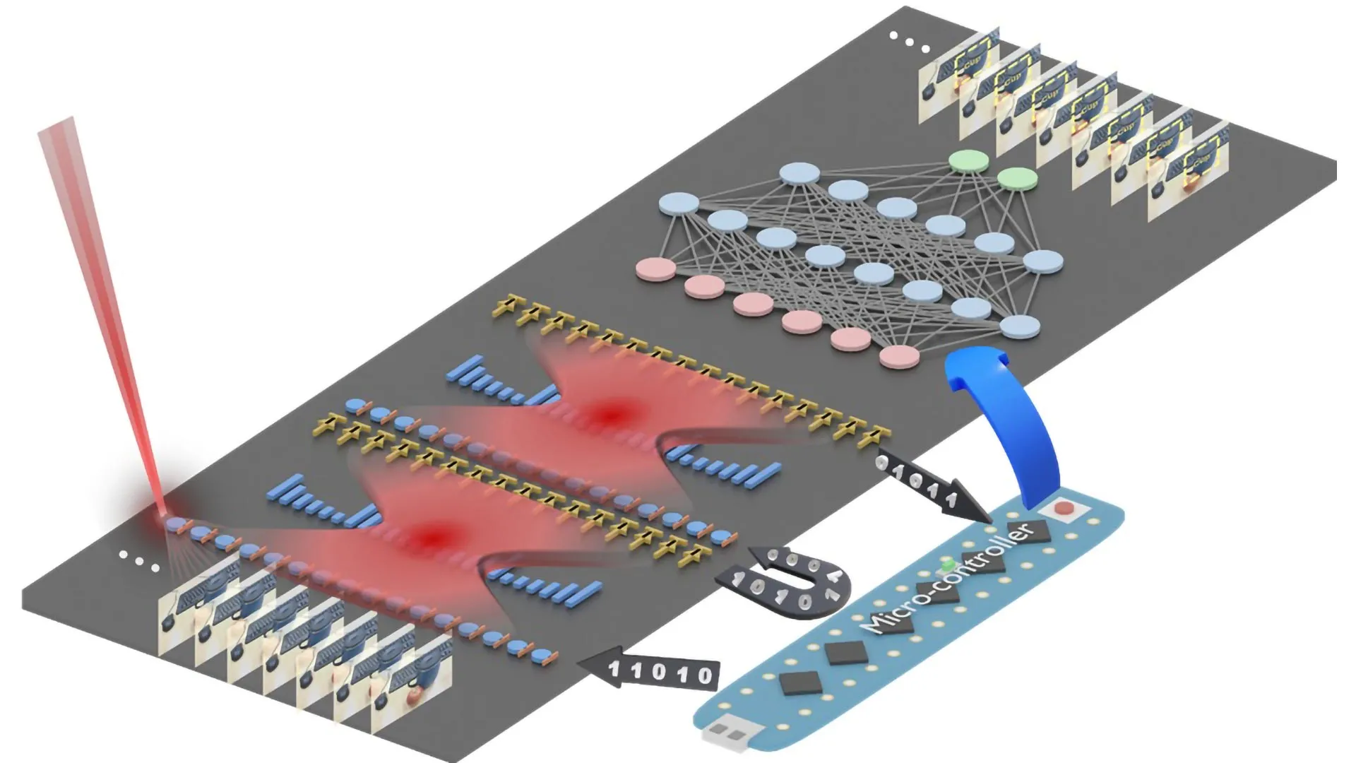
In rigorous testing, the prototype chip demonstrated remarkable proficiency, successfully classifying handwritten digits with an impressive accuracy rate of approximately 98 percent. This performance is directly comparable to that of conventional, purely electronic chips currently in use. The chip’s optical processing prowess is achieved through the strategic implementation of two sets of miniature Fresnel lenses. These lenses, which are ultrathin, flat versions of the lenses famously found in lighthouses, are fabricated using established and widely adopted semiconductor manufacturing techniques. The precision of these lenses is astonishing; each is narrower than a human hair and is directly etched onto the surface of the chip, allowing for incredibly compact and efficient light manipulation.
The operational mechanism of the chip for performing a convolution is elegantly straightforward yet highly effective. Machine learning data is initially converted into laser light on the chip. This light then traverses through the meticulously designed Fresnel lenses. These lenses, acting as sophisticated optical processors, perform the complex mathematical transformations inherent to convolution operations. Following this optical computation, the resulting light signals are converted back into digital signals, completing the AI task with unparalleled efficiency. This elegant conversion between optical and electronic domains is a testament to the researchers’ innovative approach.
Hangbo Yang, a research associate professor in Sorger’s group at UF and a key co-author of the study, highlighted the novelty of their achievement. "This is the first time anyone has put this type of optical computation on a chip and applied it to an AI neural network," Yang declared, underscoring the pioneering nature of their research in integrating optical processing directly into the core of AI neural networks. This marks a significant departure from previous attempts that may have used optical components in conjunction with, rather than as an integral part of, the processing unit.
The team further showcased the chip’s advanced capabilities by demonstrating its ability to process multiple data streams concurrently. This feat is accomplished through the ingenious application of wavelength multiplexing, a technique that leverages lasers of different colors. "We can have multiple wavelengths, or colors, of light passing through the lens at the same time," Yang explained, illustrating the inherent advantages of photonics. "That’s a key advantage of photonics." This ability to process information in parallel using different wavelengths significantly boosts the chip’s overall throughput and efficiency, making it suitable for handling increasingly complex and data-intensive AI workloads.
The collaborative spirit of scientific inquiry was evident in this research, which was conducted in close partnership with the Florida Semiconductor Institute, the University of California, Los Angeles (UCLA), and George Washington University. This interdisciplinary collaboration brought together diverse expertise, contributing to the comprehensive development and validation of the optical AI chip. Professor Sorger also pointed to the potential for swift integration of this new technology into existing AI hardware ecosystems. He noted that leading chip manufacturers such as NVIDIA are already incorporating optical elements into certain aspects of their AI systems, a trend that could significantly ease the adoption and deployment of this novel light-powered chip.
Looking towards the future, Sorger expressed a strong conviction about the trajectory of AI hardware development. "In the near future, chip-based optics will become a key part of every AI chip we use daily," Sorger predicted with confidence. He further elaborated on the imminent paradigm shift, stating, "And optical AI computing is next." This forward-looking statement suggests that the integration of optical processing into AI chips is not merely a possibility but an inevitability, poised to redefine the landscape of artificial intelligence and its energy footprint. The implications of this research are far-reaching, promising to accelerate the development of more powerful, sustainable, and accessible AI technologies that can benefit society across a multitude of domains. The reduction in energy consumption could also democratize access to advanced AI capabilities, making them more feasible for deployment in resource-constrained environments and on mobile devices. Furthermore, the speed enhancements offered by optical processing could unlock new frontiers in real-time AI applications, from autonomous systems to advanced scientific simulations. The development signifies a critical step towards a future where artificial intelligence can continue to evolve and thrive without placing an unsustainable burden on global energy resources, marking a pivotal moment in the ongoing quest for intelligent and environmentally responsible technological advancement.