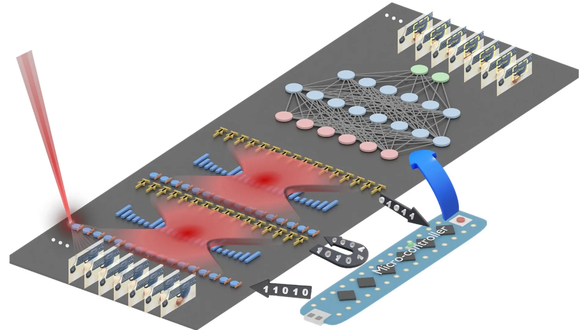
At the heart of this innovation lies the chip’s ingenious design to perform convolution operations, a fundamental and critical function within the realm of machine learning. These operations are the bedrock upon which AI systems build their ability to discern intricate patterns within vast datasets, whether they be images, video streams, or textual information. Traditionally, these convolutions demand immense computing power, translating directly into substantial energy consumption. The University of Florida team’s ingenious solution involves the direct integration of optical components onto a silicon chip, thereby creating a hybrid system that executes convolutions using precisely directed laser light and an array of microscopic lenses. This paradigm shift dramatically slashes energy consumption, achieving an efficiency boost of up to 100 times compared to conventional electronic methods, while simultaneously accelerating processing speeds.
"Performing a key machine learning computation at near zero energy is a leap forward for future AI systems," declared study leader Volker J. Sorger, the distinguished Rhines Endowed Professor in Semiconductor Photonics at the University of Florida. He emphasized the profound implications of this achievement, stating, "This is critical to keep scaling up AI capabilities in years to come." This sentiment underscores the urgent need for such advancements as AI continues its relentless march into every facet of our lives. The ability to perform complex computations with minimal energy expenditure is not merely an incremental improvement; it is a fundamental enabler for the continued, responsible growth of artificial intelligence.
The efficacy of this novel chip was rigorously tested, with the prototype demonstrating an impressive classification accuracy of approximately 98 percent when identifying handwritten digits. This level of performance is directly comparable to that of established electronic chips, proving that the pursuit of efficiency does not come at the expense of accuracy. The underlying technology relies on two sets of miniature Fresnel lenses, which are essentially flat, ultrathin replicas of the powerful lenses found in lighthouses. These lenses are meticulously fabricated using standard semiconductor manufacturing techniques, ensuring scalability and potential for widespread adoption. Remarkably, these lenses are infinitesimally small, measuring narrower than a human hair, and are etched directly onto the chip’s surface.
The operational mechanism of the chip is elegantly simple yet profoundly effective. To execute a convolution, the machine learning data is first transformed into laser light as it enters the chip. This light then traverses the meticulously arranged Fresnel lenses, which, through their precise curvature and structure, perform the necessary mathematical transformations inherent to the convolution process. Upon completion of this optical computation, the resulting light signal is converted back into a digital signal, thereby finalizing the AI task. This seamless interplay between light and silicon represents a significant departure from purely electronic processing.
"This is the first time anyone has put this type of optical computation on a chip and applied it to an AI neural network," enthused Hangbo Yang, a research associate professor in Sorger’s group at UF and a co-author of the study. This statement highlights the novelty and pioneering nature of the research, emphasizing that this is not merely an enhancement of existing technology but a fundamentally new approach to optical AI computing. The ability to integrate these optical elements directly onto a chip opens up unprecedented possibilities for miniaturization and power efficiency.
Further demonstrating the chip’s versatility and advanced capabilities, the team showcased its ability to process multiple data streams concurrently. This remarkable feat is achieved by employing lasers emitting light of different colors, a sophisticated technique known as wavelength multiplexing. "We can have multiple wavelengths, or colors, of light passing through the lens at the same time," explained Yang. "That’s a key advantage of photonics." This inherent parallelism offered by light allows for significantly higher data throughput and computational density, further amplifying the chip’s efficiency and speed.
The collaborative nature of this groundbreaking research is also noteworthy, involving a consortium of esteemed institutions including the Florida Semiconductor Institute, UCLA, and George Washington University. This interdisciplinary effort brought together diverse expertise, culminating in this significant breakthrough. Professor Sorger also pointed to the existing landscape of chip manufacturing, noting that industry giants such as NVIDIA are already incorporating optical elements into certain aspects of their AI systems. This existing infrastructure could significantly expedite the integration and adoption of this new light-powered technology.
Looking towards the horizon, Sorger expressed a clear vision for the future: "In the near future, chip-based optics will become a key part of every AI chip we use daily." He further elaborated, "And optical AI computing is next." This confident assertion suggests that the era of purely electronic AI chips may be drawing to a close, with photonics poised to take center stage. The implications are far-reaching, promising not only more efficient and sustainable AI but also enabling the development of even more powerful and sophisticated artificial intelligence systems that were previously constrained by energy limitations. The fusion of light and silicon within a single chip represents a monumental step towards a future where AI is both intelligent and environmentally responsible, powering the innovations of tomorrow without draining the resources of today. This advancement has the potential to democratize AI, making powerful computing accessible in more contexts and reducing the environmental burden associated with the rapid growth of artificial intelligence. The efficient processing of convolutions, a bottleneck in many AI applications, is now within reach of near-zero energy consumption, paving the way for a more sustainable and scalable AI ecosystem.