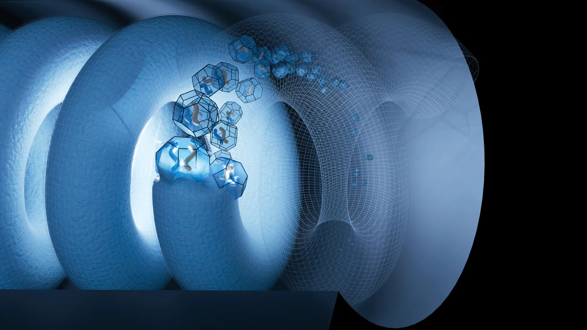
In a groundbreaking achievement, engineers have successfully developed a novel device capable of generating minuscule seismic-style vibrations, effectively shrinking the phenomenon of earthquakes down to the microscopic scale of a microchip. This remarkable breakthrough centers on a sophisticated piece of technology dubbed a surface acoustic wave phonon laser. The implications of this innovation are far-reaching, promising to pave the way for significantly more advanced chips that could dramatically enhance the capabilities of smartphones and a wide array of other wireless electronics, leading to devices that are not only smaller and faster but also consume considerably less energy.
This pioneering research was spearheaded by Matt Eichenfield, an esteemed incoming faculty member at the University of Colorado Boulder, in close collaboration with a team of accomplished scientists from the University of Arizona and Sandia National Laboratories. Their seminal findings, meticulously detailed and rigorously validated, were officially published on January 14th in the prestigious scientific journal Nature, marking a significant milestone in the field of microelectronics and wave physics.
Understanding the Fundamentals: The Nature of Surface Acoustic Waves (SAWs)
At the heart of this revolutionary new device lies the principle of surface acoustic waves, more commonly recognized by their acronym, SAWs. These waves exhibit characteristics akin to sound waves, but with a crucial distinction: instead of propagating through the bulk of a material or traversing the open air, they are confined to travel exclusively along the surface of a solid.
The destructive power of large-scale earthquakes, which generate immense surface acoustic waves that ripple across the Earth’s crust, causing widespread devastation, serves as a dramatic, albeit magnified, illustration of this phenomenon. On a much more controlled and beneficial scale, SAWs have already become indispensable components in numerous modern technologies. "SAWs devices are critical to the many of the world’s most important technologies," emphatically stated Eichenfield, who holds the distinguished Gustafson Endowed Chair in Quantum Engineering at CU Boulder and serves as the senior author of this groundbreaking new study. He further elaborated, "They’re in all modern cell phones, key fobs, garage door openers, most GPS receivers, many radar systems and more."
The Integral Role of SAWs in Powering Today’s Smartphones
Within the intricate architecture of a contemporary smartphone, SAWs play a pivotal role as highly precise filters. When radio signals are received from a cell tower, they are initially transmuted into minute mechanical vibrations. This conversion is essential for the chip’s ability to meticulously isolate the desired, useful signals from extraneous interference and ambient background noise. Once this signal purification is complete, these cleaned vibrations are then artfully reconverted back into radio waves, enabling seamless communication.
In the context of this groundbreaking study, Eichenfield and his esteemed colleagues have introduced a novel and highly effective method for generating these vital surface waves. They have achieved this through the creation of what they term a "phonon laser." While a conventional laser pointer emits light, this innovative device operates on a fundamentally different principle, producing precisely controlled mechanical vibrations. "Think of it almost like the waves from an earthquake, only on the surface of a small chip," explained Alexander Wendt, a dedicated graduate student at the University of Arizona and the lead author of the study, drawing a vivid analogy to illustrate the device’s function.
A significant limitation of most existing SAW systems is their reliance on two separate chips and an external power source. The revolutionary new design ingeniously consolidates all necessary components onto a single chip. Furthermore, it boasts the potential to operate efficiently using only a standard battery, while simultaneously achieving vastly higher operating frequencies, representing a substantial leap forward in miniaturization and performance.
Deconstructing the "Phonon Laser": A Novel Approach to Vibration Generation
To fully appreciate the ingenuity of this new device, it is beneficial to first understand the underlying principles of how conventional lasers function. Many commonly encountered lasers, such as diode lasers, operate by generating light through a process of reflection. Tiny mirrors strategically placed on a semiconductor chip cause light to bounce back and forth. As the light repeatedly reflects, it interacts with energized atoms within the semiconductor. These energized atoms, in turn, release additional light, thereby amplifying and strengthening the emitted beam.
"Diode lasers are the cornerstone of most optical technologies because they can be operated with just a battery or simple voltage source, rather than needing more light to create the laser like a lot of previous kinds of lasers," Eichenfield remarked, highlighting the practical advantages of this technology. He continued, "We wanted to make an analog of that kind of laser but for SAWs." This ambition directly fueled the development of the phonon laser.
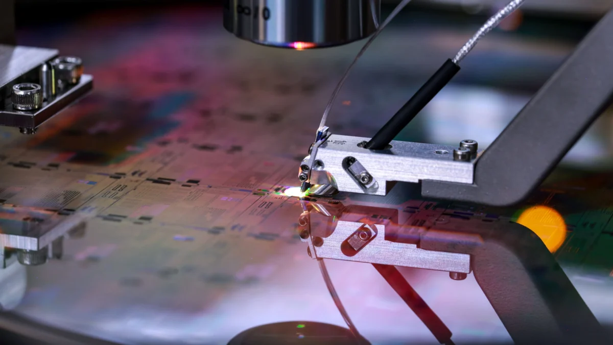
To realize this vision, the research team meticulously engineered a bar-shaped device, measuring approximately half a millimeter in length – a testament to the miniaturization achieved.
A Sophisticated Architecture: The Layered Composition of the Device
The sophisticated design of the phonon laser is a result of the precise layering of several specialized materials, each contributing unique properties to the overall functionality. At the very base of this intricate structure lies silicon, the ubiquitous and foundational material that forms the backbone of most modern computer chips. Situated directly above the silicon is a remarkably thin layer of lithium niobate, a material renowned for its piezoelectric properties. Piezoelectric materials possess the extraordinary ability to generate oscillating electric fields when subjected to mechanical vibrations, and conversely, to vibrate when exposed to oscillating electric fields.
The uppermost layer, an extremely thin sheet of indium gallium arsenide, possesses highly unusual electronic properties. This material is capable of accelerating electrons to exceptionally high speeds, even under the influence of relatively weak electric fields.
In concert, these precisely layered materials facilitate a direct and highly efficient interaction between the surface acoustic waves propagating along the lithium niobate surface and the fast-moving electrons within the indium gallium arsenide layer. This synergy is the key to the phonon laser’s operation.
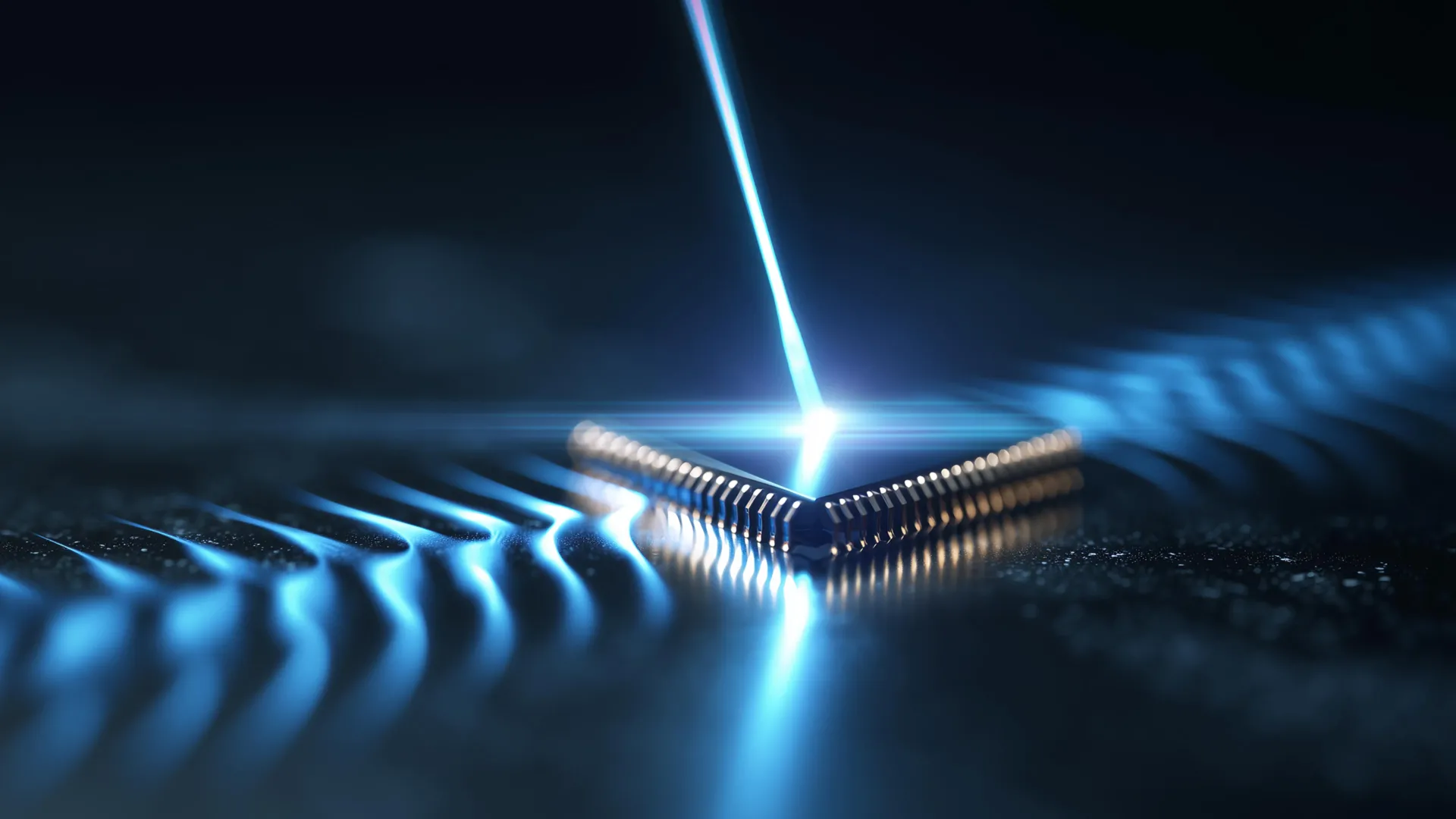
Orchestrating Vibrations: The Laser-Like Mechanism of Wave Amplification
The researchers liken the operational mechanism of this novel device to that of a wave pool, where waves are generated and amplified. When an electric current is introduced and flows through the indium gallium arsenide layer, it instigates the formation of surface waves within the lithium niobate layer. These waves then embark on a journey, traveling forward until they encounter a carefully designed reflector. Upon striking the reflector, they are propelled backward, mirroring the behavior of light reflecting between mirrors in a conventional laser cavity.
Crucially, each forward passage of the wave results in a strengthening of its amplitude, while each backward pass leads to a diminishment of its power. "It loses almost 99% of its power when it’s moving backward, so we designed it to get a substantial amount of gain moving forward to beat that," explained Wendt, detailing the engineering challenge and its ingenious solution. Through these repeated cycles of forward amplification and backward loss, the vibrations progressively grow in intensity. Eventually, they achieve a critical strength, allowing a portion of this amplified vibrational energy to escape from one side of the device, analogous to how laser light eventually exits its optical cavity.
The Dawn of Faster Waves and Ultra-Compact Devices
Employing this innovative approach, the research team has successfully generated surface acoustic waves vibrating at an impressive frequency of approximately 1 gigahertz, which translates to billions of oscillations per second. Furthermore, the researchers express strong confidence that the same fundamental design principles could be further refined and scaled to achieve frequencies in the tens or even hundreds of gigahertz.
This represents a substantial advancement over traditional SAW devices, which typically reach their operational limit at around 4 gigahertz, rendering the new system significantly faster and more capable. Eichenfield articulated the profound potential of this breakthrough, stating that it could usher in an era of wireless devices that are not only smaller and more powerful but also remarkably more energy-efficient.
In the current generation of smartphones, a complex and often power-intensive process is required for signal processing. Multiple chips are involved in the repeated conversion of radio waves into SAWs and back again, a cycle that occurs every time a user sends a message, makes a call, or browses the internet. The ultimate ambition of this research team is to drastically simplify this process by developing a single, integrated chip that can efficiently handle all essential signal processing functions using only surface acoustic waves.
"This phonon laser was the last domino standing that we needed to knock down," Eichenfield concluded, emphasizing the pivotal nature of this invention. "Now we can literally make every component that you need for a radio on one chip using the same kind of technology." This sentiment underscores the transformative potential of the phonon laser, heralding a future where highly integrated and efficient wireless communication systems become a widespread reality, fundamentally reshaping the landscape of portable electronics.