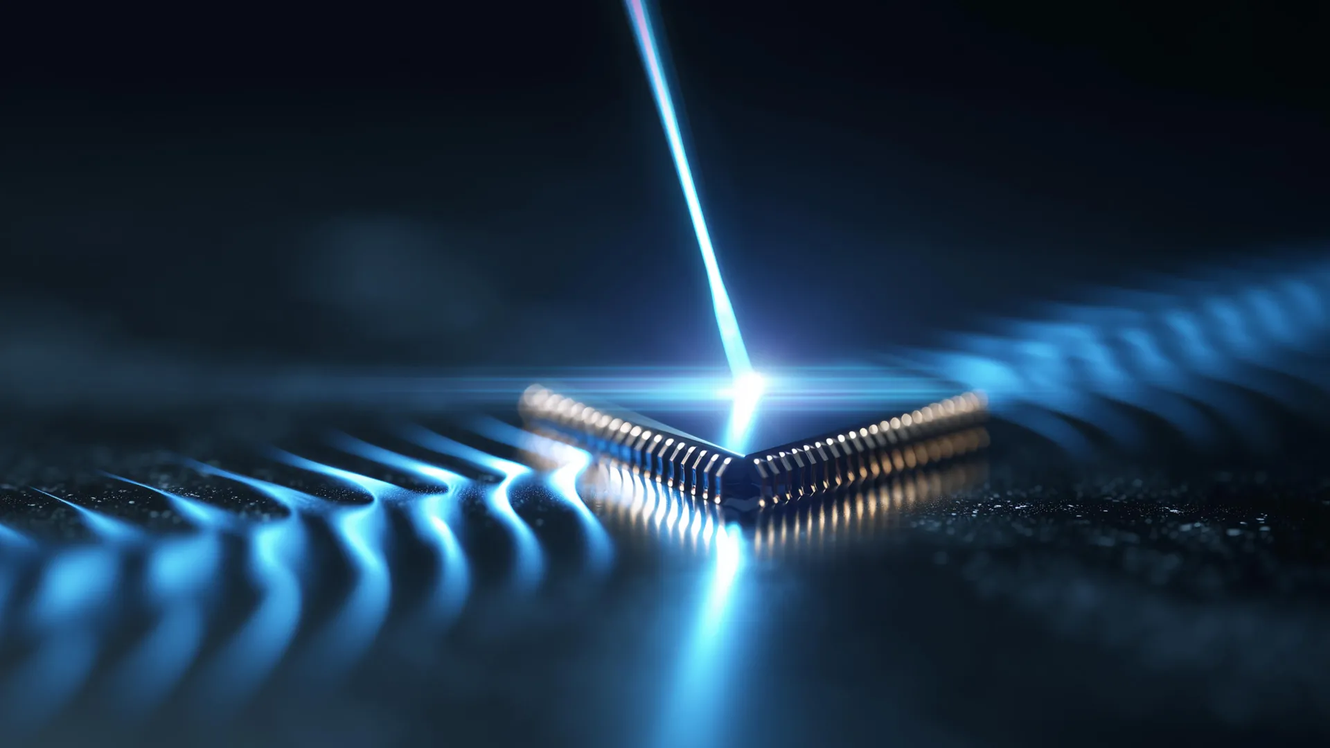
At the heart of this innovation lies a device that harnesses what are known as surface acoustic waves, or SAWs. These are not your typical sound waves that travel through air; instead, they are mechanical vibrations that propagate exclusively along the surface of a material. While massive earthquakes on Earth generate SAWs on a colossal scale, causing widespread devastation, these same principles, miniaturized to an astonishing degree, are already indispensable in our modern technological landscape.
"SAWs devices are critical to the many of the world’s most important technologies," emphasized Matt Eichenfield, a senior author of the study and the newly appointed Gustafson Endowed Chair in Quantum Engineering at CU Boulder. "They’re in all modern cell phones, key fobs, garage door openers, most GPS receivers, many radar systems and more." Indeed, within the intricate circuitry of a smartphone, SAWs play a crucial role as highly precise filters. When radio signals arrive from a cell tower, they are ingeniously converted into minute mechanical vibrations. This conversion allows the chips to meticulously separate desired signals from unwanted interference and background noise. Once the signal is purified, these vibrations are then reconverted back into radio waves for further processing.
The breakthrough presented in this study lies in a novel method developed by Eichenfield and his team to generate these surface waves: the "phonon laser." While a conventional laser emits light, this innovative device produces controlled mechanical vibrations, akin to miniature seismic events confined to the surface of a microchip. "Think of it almost like the waves from an earthquake, only on the surface of a small chip," explained Alexander Wendt, a graduate student at the University of Arizona and the lead author of the research.
A key advantage of this new phonon laser design is its ability to integrate multiple functionalities onto a single chip. Current SAW systems often require two separate chips and an external power source. In stark contrast, the newly developed phonon laser consolidates these functions into a single, compact unit that can operate efficiently using just a battery, and critically, achieve much higher operating frequencies.
To grasp the ingenuity of the phonon laser, it’s helpful to draw a parallel with conventional lasers. Many everyday lasers, such as those found in laser pointers or CD players, are diode lasers. These operate by generating light through a process of reflection between two tiny mirrors embedded within a semiconductor chip. As light bounces back and forth between these mirrors, it interacts with energized atoms, stimulating them to release more light, thereby amplifying the beam.
"Diode lasers are the cornerstone of most optical technologies because they can be operated with just a battery or simple voltage source, rather than needing more light to create the laser like a lot of previous kinds of lasers," Eichenfield explained. "We wanted to make an analog of that kind of laser but for SAWs." The team successfully engineered a bar-shaped device, approximately half a millimeter in length, to achieve this goal.
The construction of this remarkable phonon laser involves a sophisticated layering of specialized materials. The foundation of the device is silicon, the ubiquitous material that forms the bedrock of most computer chips. Perched atop the silicon is a thin film of lithium niobate, a material renowned for its piezoelectric properties. When lithium niobate is subjected to mechanical stress or vibration, it generates oscillating electric fields, and conversely, these electric fields can induce vibrations in the material itself. The uppermost layer is an exceptionally thin sheet of indium gallium arsenide. This material possesses unique electronic characteristics, enabling electrons to accelerate to very high speeds even under relatively weak electric fields.
The synergistic interplay between these layered materials is what enables the phonon laser to function. Vibrations traveling along the surface of the lithium niobate layer directly interact with the high-speed electrons within the indium gallium arsenide. This interaction is the crucial element that allows for the amplification of SAWs, mirroring the light amplification process in a conventional laser.
The researchers liken the operational principle of their phonon laser to that of a wave pool. When an electric current is passed through the indium gallium arsenide layer, surface waves are initiated in the lithium niobate. These waves propagate forward, encounter a carefully designed reflector, and then bounce back. This continuous cycle of forward and backward travel is analogous to light reflecting between mirrors in an optical laser. Each forward journey of the wave is designed to amplify its energy, while the backward journey is engineered to minimize energy loss.
"It loses almost 99% of its power when it’s moving backward, so we designed it to get a substantial amount of gain moving forward to beat that," Wendt elaborated. After undergoing numerous such amplification cycles, the vibrations grow sufficiently strong that a portion of this energy is emitted from one side of the device, much like a laser beam exits its optical cavity.
The immediate and most impactful consequence of this phonon laser technology is its potential to significantly increase the operating frequency of SAW devices. The research team successfully generated surface acoustic waves vibrating at approximately 1 gigahertz, which translates to billions of oscillations per second. Furthermore, they are confident that the underlying design can be further optimized to achieve frequencies in the tens or even hundreds of gigahertz. This represents a substantial leap forward, as traditional SAW devices typically reach their performance ceiling at around 4 gigahertz.
The implications for the consumer electronics market are immense. Eichenfield predicts that this advancement will usher in an era of wireless devices that are not only smaller in size but also boast enhanced processing power and vastly improved energy efficiency. He points to the current architecture of smartphones, where multiple chips are employed to repeatedly convert radio waves into SAWs and back again for tasks like sending messages, making calls, or browsing the internet. The ultimate goal of Eichenfield’s team is to streamline this process by developing a single, integrated chip capable of handling all necessary signal processing using the sophisticated principles of surface acoustic waves.
"This phonon laser was the last domino standing that we needed to knock down," Eichenfield declared with evident satisfaction. "Now we can literally make every component that you need for a radio on one chip using the same kind of technology." This sentiment underscores the transformative potential of their work, marking a significant milestone in the quest for miniaturized, high-performance electronic devices that will redefine the capabilities of our everyday technology. The era of the ultra-compact, hyper-efficient smartphone, powered by microscopic vibrations, is now a tangible reality on the horizon.