The observed light-induced atomic motion is particularly pronounced in a specialized class of TMDs known as Janus materials. These materials earn their evocative name from Janus, the Roman god of transitions, owing to their unique asymmetric structure. This inherent asymmetry imbues them with a heightened sensitivity to light and external forces, making them ideal candidates for applications that leverage optical signals over traditional electrical currents. The potential implications are far-reaching, promising to revolutionize fields such as computing, sensing, and optoelectronics by enabling faster, cooler computer chips, more responsive sensors, and flexible, light-driven systems.
"In the realm of nonlinear optics, light possesses the remarkable ability to be reshaped, enabling the generation of new colors, the creation of faster light pulses, and the development of optical switches that can control the flow of information by turning signals on and off," explained Kunyan Zhang, a doctoral alumna of Rice University and the first author of the study. "The advent of two-dimensional materials, which are astonishingly thin, only a few atoms thick, has made it possible to engineer these sophisticated optical tools on an incredibly small scale."
The Unique Architecture of Janus Materials: A Foundation for Light Sensitivity
Transition metal dichalcogenides (TMDs) are a class of layered materials characterized by a central layer of a transition metal, such as molybdenum, sandwiched between two layers of a chalcogen element, like sulfur or selenium. This layered structure, combined with their inherent properties of electrical conductivity, potent light absorption capabilities, and remarkable mechanical flexibility, has propelled them to the forefront as key contenders for the development of next-generation electronic and optical devices.
However, within this diverse family of TMDs, Janus materials distinguish themselves through a unique structural characteristic: their top and bottom atomic layers are not identical but are instead composed of different chemical elements. This deliberate elemental disparity results in an intrinsic asymmetry within the material’s atomic lattice. This asymmetry is not merely a structural curiosity; it gives rise to a built-in electrical polarity, a fundamental property that significantly amplifies their sensitivity to external stimuli, most notably light and mechanical forces.
"Our research delves into the intricate relationship between the structural makeup of Janus materials and their optical behavior," Zhang elaborated. "Crucially, we are investigating how light itself can act as a direct source of force within these materials, inducing physical changes at the atomic level."
Illuminating Atomic Movement: Laser Light as a Precision Tool
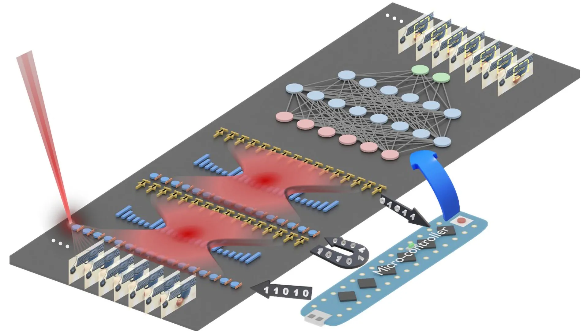
To meticulously investigate this intriguing phenomenon, the research team employed a sophisticated experimental setup utilizing laser beams of various wavelengths. They focused their attention on a specific two-layer Janus TMD material, ingeniously constructed from a stack of molybdenum sulfur selenide layered atop molybdenum disulfide. The researchers then probed the material’s response by observing how it interacted with and altered incoming light. A key technique employed was second harmonic generation (SHG). SHG is a nonlinear optical process where a material, when exposed to incident light of a certain frequency, emits light at precisely double that frequency.
The critical observation emerged when the frequency of the incoming laser beam was precisely tuned to match the material’s natural resonant frequencies. Under these specific conditions, the typical, predictable SHG pattern produced by the material became noticeably distorted. This distortion was not random; it served as a telltale indicator that the atoms within the material were physically shifting their positions.
"We made a significant discovery: when we shine light on Janus molybdenum sulfur selenide and molybdenum disulfide, it generates tiny, yet distinctly directional forces within the material," Zhang reported. "These internal forces manifest themselves as observable changes in the material’s SHG pattern. Normally, the SHG signal forms a highly symmetrical, six-pointed ‘flower’ shape, a direct reflection of the crystal’s inherent symmetry. However, when light exerts its force on the atoms, this symmetry is disrupted – the petals of the SHG pattern begin to shrink unevenly, providing visual evidence of atomic displacement."
Optostriction and Layer Coupling: The Underlying Mechanisms
The researchers meticulously traced the origin of these observed SHG distortions to a phenomenon known as optostriction. Optostriction is a fascinating process where the electromagnetic field of light itself exerts a mechanical force on the atoms within a material, causing them to move. In the case of Janus materials, the unique layered structure and the strong coupling that exists between these layers play a pivotal role in amplifying this optostrictive effect. This enhanced coupling means that even extremely minuscule forces, generated by the light, can produce measurable strain within the material.
"Janus materials are exceptionally well-suited for this type of investigation precisely because their uneven elemental composition fosters an enhanced interaction and coupling between their constituent layers," Zhang explained. "This enhanced coupling renders them significantly more sensitive to the subtle forces exerted by light – forces that are so infinitesimally small that they would be exceedingly difficult to measure directly. However, by observing the changes in the SHG signal pattern, we can indirectly but reliably detect and quantify these atomic movements."
A Glimpse into the Future: Unlocking the Potential of Optical Technologies
The profound sensitivity exhibited by Janus materials to light-induced atomic forces holds immense promise for their integration into a wide array of future optical technologies. Devices designed to actively guide or control the flow of light through this light-induced mechanical manipulation could pave the way for the development of photonic chips that operate at significantly higher speeds and consume far less energy compared to their traditional electronic counterparts. This is because light-based circuits generate considerably less heat than electrical circuits, a critical factor for advancing energy efficiency in computing.
Beyond computing, these unique properties could be harnessed to create highly sophisticated sensors capable of detecting extremely subtle vibrations or minute pressure variations. Furthermore, this controllable light-matter interaction could be instrumental in developing adjustable light sources for advanced display technologies and cutting-edge imaging systems, offering unprecedented levels of precision and adaptability.
"The ability to actively control these materials with light opens up exciting possibilities for designing next-generation photonic chips, ultrasensitive detectors, and even quantum light sources," stated Shengxi Huang, an associate professor of electrical and computer engineering and materials science and nanoengineering at Rice. Huang, who is also affiliated with prestigious Rice institutes including the Smalley-Curl Institute, the Rice Advanced Materials Institute, and the Ken Kennedy Institute, added, "These are technologies that rely on light to carry and process information, rather than the conventional reliance on electricity, promising a paradigm shift in how we approach information technology."
The Profound Impact of Subtle Structural Asymmetries
In essence, this groundbreaking research demonstrates a fundamental principle: even seemingly minor structural imbalances within materials can unlock significant technological opportunities. By revealing how the inherent internal asymmetry of Janus TMDs provides a novel and powerful means to influence and control the behavior of light, the study underscores the importance of exploring subtle structural nuances in the design of advanced materials. This work not only deepens our understanding of light-matter interactions at the nanoscale but also provides a tangible roadmap for engineering the materials of the future, paving the way for a more efficient, responsive, and light-centric technological landscape.
The research was generously supported by funding from multiple esteemed organizations, including the National Science Foundation (grants 2246564 and 1943895), the Air Force Office of Scientific Research (grant FA9550-22-1-0408 and FA2386-24-1-4049), the Welch Foundation (grant C-2144), the U.S. Department of Energy (grants DE-SC0020042 and DE-AC02-05CH11231), and the Taiwan Ministry of Education. The views and conclusions presented in this article are solely the responsibility of the authors and do not necessarily reflect the official policies or opinions of the funding organizations and institutions involved.