
 Imroatul Nasiyah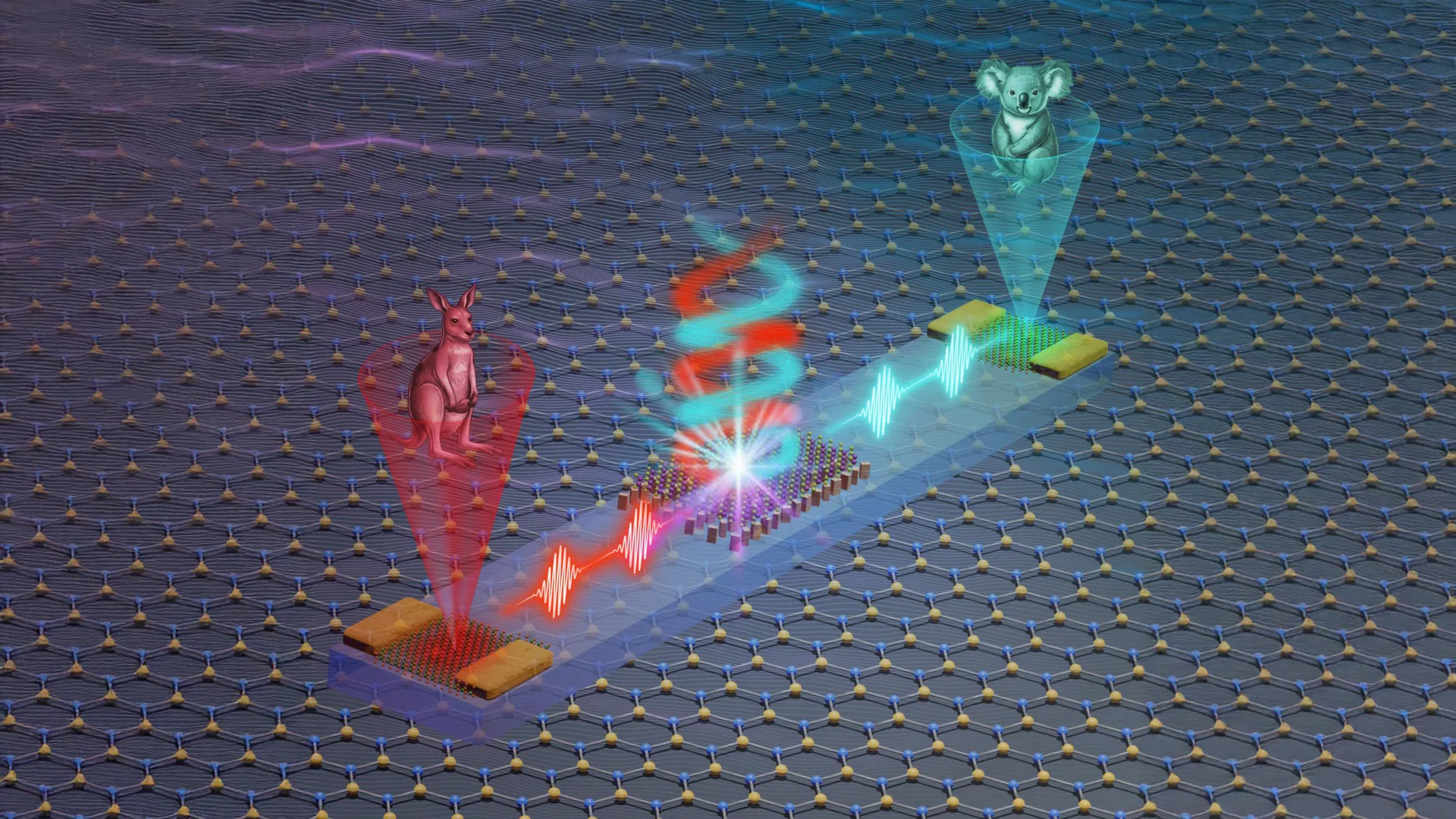
The research, spearheaded by a dedicated team from the Monash School of Physics and Astronomy, masterfully combines sophisticated nanotechnology with state-of-the-art materials. Their innovative approach has successfully overcome a critical bottleneck that has limited the field for years, enabling the creation of a fully integrated chip. For the very first time, this compact system possesses the remarkable ability to produce highly specialized light signals, meticulously guide them along predetermined paths, and then efficiently convert them into electrical signals—all within the confines of a single, unified device. The information stored and manipulated by this chip leverages a unique quantum property known as the "valley degree of freedom." Researchers are immensely optimistic that this distinctive characteristic will unlock entirely novel paradigms for encoding, transmitting, and processing data, potentially leading to computational capabilities far beyond current limitations.
The publication of these transformative findings in the prestigious journal Nature Photonics highlights the significance of this achievement. Lead author Dr. Chi Li emphasized the pivotal role this development plays in overcoming a substantial hurdle in valleytronics research. "Until now," Dr. Li explained, "we could either generate or detect these signals, but the capability to perform all these functions within a single integrated device was absent. What we have successfully engineered is a comprehensive on-chip system that possesses the precision to create, route, and read this information with exceptional accuracy."
The intricate design of this novel device hinges on the utilization of ultra-thin materials, some measuring only a few atoms in thickness. These exotic materials are meticulously paired with specially engineered nanostructures, which are critical for precisely controlling light at extraordinarily small scales. Dr. Kaijian Xing, a co-first author of the study and a Research Fellow at Monash University, elaborated on the practical ingenuity of the team’s integration method. "We have adopted a straightforward stacking approach," Dr. Xing stated, "to seamlessly integrate these ultra-thin materials with metasurfaces. This technique effectively circumvents the inherent technical difficulties associated with directly growing materials on photonic structures, thereby paving the way for even more profound advancements in valleytronics."
A particularly compelling advantage of this cutting-edge technology is its operational capability at room temperature. Many existing quantum systems necessitate extremely low temperatures, a requirement that significantly complicates their implementation and escalates costs for real-world applications. The ability to function at ambient temperatures drastically enhances the practicality and accessibility of this new photonic technology.
Senior author Dr. Haoran Ren, an ARC Future Fellow and the driving force behind the Monash NanoMeta Group, articulated the far-reaching implications of this work. He believes that this breakthrough could be instrumental in ushering in a new era of compact photonic devices that are not only highly programmable but also remarkably energy-efficient. Dr. Ren further elaborated on the potential applications, suggesting that this technology could underpin the development of significantly faster computing systems, lead to substantial reductions in energy consumption, and enable entirely new methodologies for secure communications and sophisticated data processing. "This represents a substantial stride towards the realization of scalable, chip-based technologies that harness the power of light, rather than electricity, for information processing," Dr. Ren affirmed. He elaborated on the inherent advantages of photonic devices, noting their capacity for achieving immense bandwidths, facilitating ultra-fast data transmission, and minimizing energy usage. Consequently, the achievements of his team hold immense promise for applications spanning quantum computing, advanced imaging techniques, and the next generation of optical communication systems.
To underscore the versatility and power of the chip, the research team successfully demonstrated its ability to encode and process two distinct images concurrently. This experimental validation clearly illustrated the device’s capacity to manage multiple streams of information simultaneously, a critical feature for the advancement of future computing architectures.
Professor Stefan A. Maier, Head of the School of Physics and Astronomy and Director of the Nanophotonics Laboratory at Monash University, highlighted the significance of this development in bridging the gap between fundamental scientific discoveries and tangible technological applications. "This is a crucial step towards the creation of fully integrated valleytronic systems," Professor Maier commented. "By ingeniously merging light and quantum materials on a single chip, we are unlocking new and powerful ways to encode and process information."
The collaborative nature of this groundbreaking project is also noteworthy, involving a diverse international consortium of researchers. Experts in nanophotonics, two-dimensional materials, and optoelectronics from Australia, China, Singapore, Germany, and Japan converged their knowledge and skills to bring this ambitious endeavor to fruition. The core Monash University team comprised Dr. Chi Li, Dr. Kaijian Xing, Professor Michael S. Fuhrer, Professor Stefan A. Maier, and Dr. Haoran Ren. Significant contributions to the project were also provided by researchers from the Singapore University of Technology and Design, LMU Munich, and the University of Technology Sydney, underscoring the global impact and collaborative spirit driving this revolutionary advancement in photonic computing.