As the digital world expands at an unprecedented rate, so does the need for memory technologies that can handle increasing data loads with remarkable speed and minimal power draw. Existing memory solutions, while capable, often struggle to meet the stringent requirements of next-generation devices, which are expected to be more powerful, more interconnected, and more sustainable. The University of Minnesota team’s work on Ni₂W offers a compelling alternative and a powerful complement to current technologies, paving the way for a future where our electronic devices are not only smarter but also significantly greener.
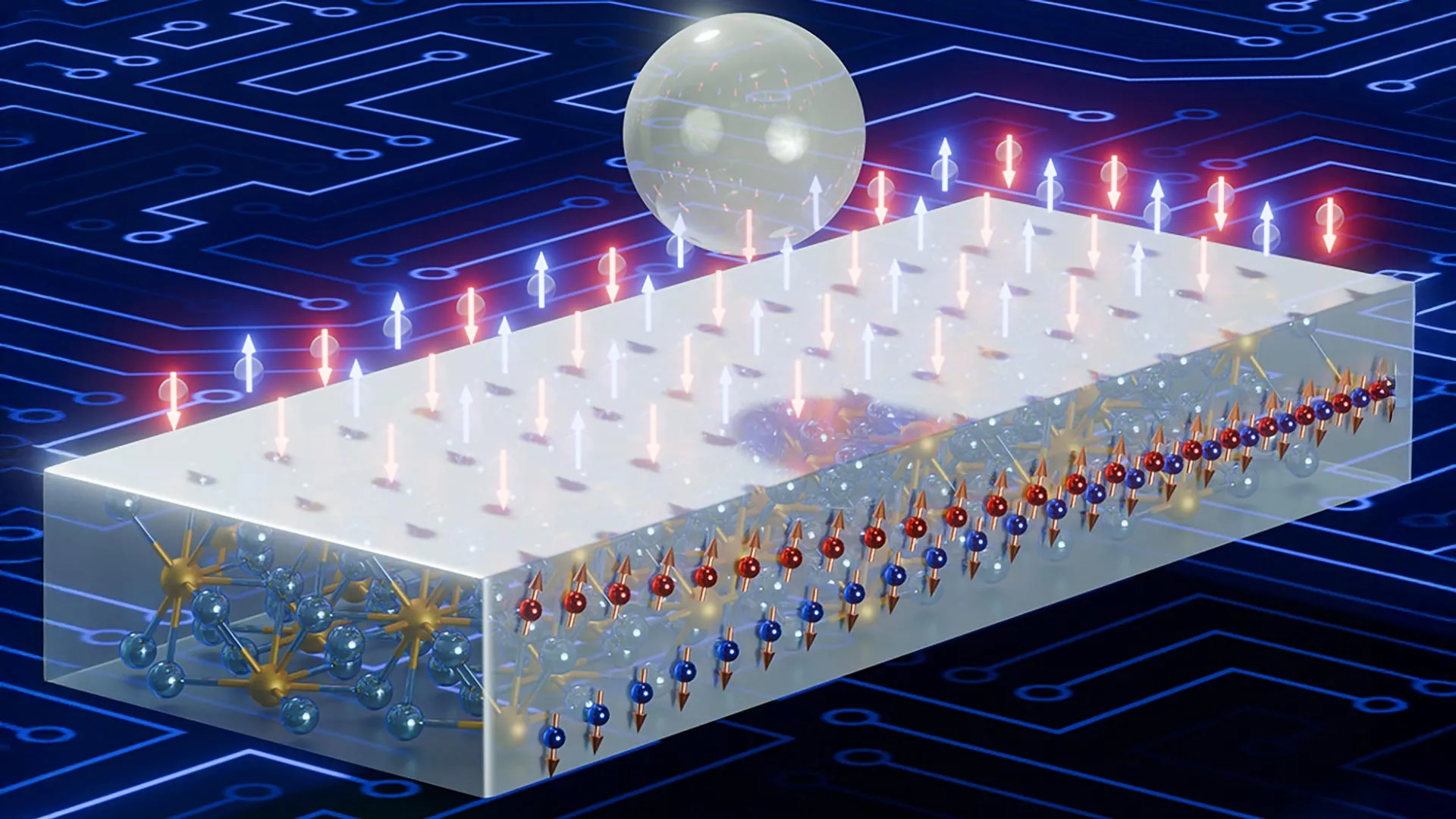
At the heart of this innovation lies Ni₂W, a meticulously engineered material composed of nickel and tungsten. The researchers discovered that this low-symmetry alloy possesses an extraordinary ability to generate a potent phenomenon known as spin-orbit torque (SOT). SOT is a critical mechanism in spintronics, a field of physics and engineering that focuses on the intrinsic spin of electrons, in addition to their charge, in solid-state devices. Manipulating this spin is key to developing novel memory and logic technologies that can surpass the limitations of conventional electronics.
"Ni₂W reduces power usage for writing data, potentially cutting energy use in electronics significantly," stated Jian-Ping Wang, a distinguished senior author of the paper and a leading figure in the Department of Electrical and Computer Engineering (ECE) at the University of Minnesota Twin Cities. This reduction in power consumption for data writing is a pivotal aspect of the discovery. In traditional memory technologies, writing data involves physically moving electrons or changing their charge, processes that can be energy-intensive. SOT, on the other hand, leverages the quantum mechanical property of electron spin to manipulate magnetic states, a far more efficient approach.
The implications of this research are far-reaching, with the potential to dramatically reduce the electricity consumption of a wide array of electronic devices. From the smartphones in our pockets to the massive data centers that power the internet, the ability to write data with significantly less energy could lead to a substantial decrease in global electricity usage. This not only translates to lower energy bills but also contributes to a more sustainable technological ecosystem, a critical concern in an era of climate change. Imagine smartphones that last days on a single charge, or data centers that operate with a fraction of their current energy footprint – this is the future Ni₂W could help usher in.
What sets Ni₂W apart from conventional materials is its remarkable ability to generate spin currents in multiple directions. This unique characteristic enables "field-free" switching of magnetic states, meaning the material can change its magnetic orientation without the need for external magnetic fields. This is a significant advancement because external magnetic fields, often generated by large and power-hungry electromagnets, have been a bottleneck in miniaturizing and improving the energy efficiency of magnetic memory devices.
"We observed high SOT efficiency with multi-direction in Ni₂W both on its own and when layered with tungsten, pointing to its strong potential for use in low-power, high-speed spintronic devices," explained Yifei Yang, a fifth-year Ph.D. student in Professor Wang’s group and a co-first author of the paper. The ability to achieve efficient SOT switching in multiple directions without external fields is a crucial enabler for creating smaller, faster, and more power-efficient spintronic devices. This multi-directional control opens up new avenues for designing complex logic circuits and ultra-dense memory arrays.
Another significant advantage of Ni₂W is its accessibility and manufacturability. The material is composed of common, abundant metals and can be produced using standard industrial processes. This ease of production makes it highly attractive to industry partners looking for scalable and cost-effective solutions. The potential for Ni₂W to be implemented into everyday technology like smartwatches, phones, and other portable devices is now a tangible reality, promising to bring about a new generation of smarter and more sustainable gadgets. The prospect of integrating this advanced material into devices we use daily, without significant manufacturing hurdles or prohibitive costs, accelerates its potential impact.
The research team’s findings were further validated by computational analysis. "We are very excited to see that our calculations confirmed the choice of the material and the SOT experimental observation," remarked Seungjun Lee, a postdoctoral fellow in ECE and the co-first author of the paper. This synergy between theoretical prediction and experimental verification strengthens the confidence in the robustness of the discovery and its potential for practical application. The confirmation through computational modeling not only validates the experimental results but also provides a deeper understanding of the underlying physics governing the material’s behavior, which can guide future research and development.
The next phase of this research involves scaling down the technology. The team plans to grow these Ni₂W materials into even smaller devices than previously achieved, further pushing the boundaries of miniaturization and performance. This incremental yet critical step is essential for translating laboratory discoveries into commercially viable products that can be integrated into the intricate architectures of modern electronics. The pursuit of smaller device dimensions is a relentless endeavor in the semiconductor industry, and the ability to achieve this with an energy-efficient material like Ni₂W is a significant stride forward.
The collaborative nature of this groundbreaking research is evident in the extensive list of contributors. Beyond Professors Wang and Low, and students Yang and Lee, the ECE team included Yu-Chia Chen, Qi Jia, Brahmudutta Dixit, Duarte Sousa, Yihong Fan, Yu-Han Huang, Deyuan Lyu, and Onri Jay Benally. Crucially, the project also benefited from the expertise of Michael Odlyzko, Javier Garcia-Barriocanal, Guichuan Yu, and Greg Haugstad from the University of Minnesota Characterization Facility, as well as Zach Cresswell and Shuang Liang from the Department of Chemical Engineering and Materials Science. This multidisciplinary approach, drawing on diverse expertise, is often the hallmark of significant scientific breakthroughs.
This pioneering work was generously supported by several key organizations. The SMART (Spintronic Materials for Advanced Information Technologies) initiative, a world-leading research center dedicated to advancing spin-based computing and memory systems, played a vital role. SMART, as one of seven centers under the nCORE (next-generation Computation and Communication Electronic Systems) program, sponsored by the Semiconductor Research Corporation and the National Institute of Standards and Technology, fosters cutting-edge research in this domain. Furthermore, the Global Research Collaboration Logic and Memory program provided crucial funding, underscoring the importance of this research on a national and international scale. The collaboration also involved the University of Minnesota Characterization Facility and the Minnesota Nano Center, providing essential resources and infrastructure for the successful execution of the study. The collective effort and support from these entities highlight the strategic importance of developing next-generation electronic materials.