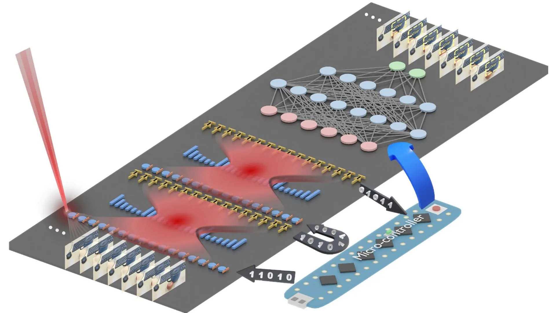
At the heart of this innovation lies a chip meticulously engineered to perform convolution operations. These operations are fundamental to the functioning of machine learning, serving as the engine that enables AI systems to discern intricate patterns within vast datasets, including images, video streams, and textual information. Historically, these convolution operations have been computationally intensive, requiring substantial processing power and, consequently, significant energy consumption. The UF team’s ingenious approach integrates optical components directly onto a standard silicon chip, creating a hybrid system that executes convolutions using focused laser light and precisely calibrated microscopic lenses. This paradigm shift dramatically slashes energy consumption and concurrently accelerates processing speeds, offering a dual benefit for AI development.
"Performing a key machine learning computation at near zero energy is a leap forward for future AI systems," stated Professor Volker J. Sorger, the study’s lead researcher and the distinguished Rhines Endowed Professor in Semiconductor Photonics at the University of Florida. He emphasized the critical importance of this development, asserting, "This is critical to keep scaling up AI capabilities in years to come." This statement underscores the profound implications of their work for the continued advancement and widespread adoption of AI technologies across diverse sectors.
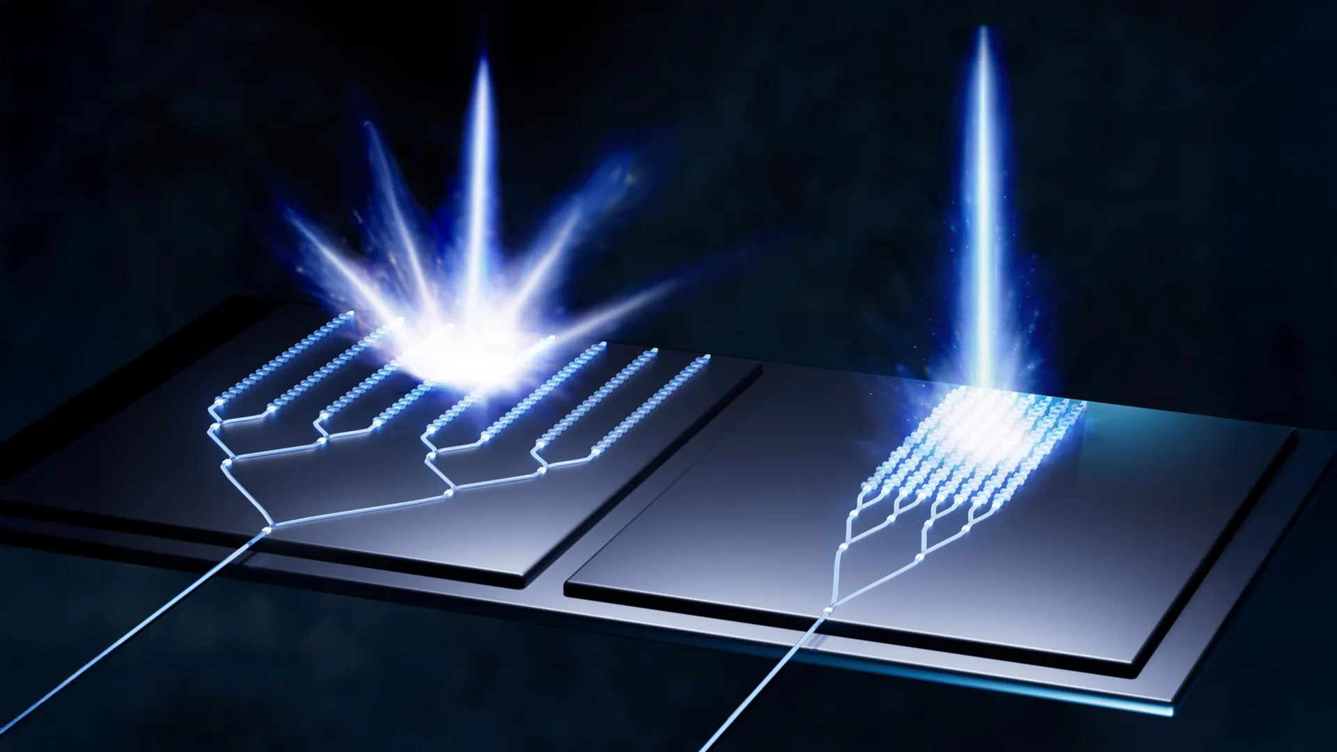
In rigorous testing, the prototype chip demonstrated remarkable proficiency, achieving an impressive classification accuracy of approximately 98 percent when identifying handwritten digits. This performance is directly comparable to that of conventional electronic chips, proving that optical computation can rival, and in some aspects surpass, established methods. The system ingeniously employs two sets of miniature Fresnel lenses, which are essentially flat, ultrathin versions of the powerful lenses famously used in lighthouses. These specialized lenses are fabricated using established semiconductor manufacturing techniques, ensuring scalability and compatibility with existing industry processes. Each lens is incredibly small, narrower than a human hair, and is directly etched onto the surface of the chip, showcasing the precision and miniaturization achieved by the researchers.
The process by which the chip performs a convolution involves a sophisticated conversion of machine learning data into laser light once it enters the chip. This light then traverses the array of Fresnel lenses, which are meticulously designed to perform the complex mathematical transformations inherent in convolution. The outcome of this optical computation is subsequently converted back into a digital signal, thereby completing the AI task. This elegant conversion between light and electrical signals allows for the leverage of photonics’ inherent advantages while seamlessly integrating with the digital infrastructure of AI systems.
Hangbo Yang, a research associate professor within Professor Sorger’s group at UF and a co-author of the study, highlighted the novelty of their achievement: "This is the first time anyone has put this type of optical computation on a chip and applied it to an AI neural network." This statement emphasizes the groundbreaking nature of their research, pushing the boundaries of what is currently possible in optical AI computing.
Further demonstrating the versatility and power of their design, the team also showcased the chip’s ability to process multiple data streams concurrently. This remarkable feat is accomplished by employing lasers of different colors, a technique known as wavelength multiplexing. "We can have multiple wavelengths, or colors, of light passing through the lens at the same time," explained Yang, elaborating on a key advantage of photonic systems. "That’s a key advantage of photonics." This capability allows for significantly increased data throughput and computational density, further amplifying the chip’s efficiency.
This ambitious research was not an isolated effort but rather a testament to collaborative innovation. The project was conducted in close partnership with leading institutions including the Florida Semiconductor Institute, the University of California, Los Angeles (UCLA), and George Washington University. Professor Sorger pointed to the existing integration of optical elements in some AI systems by major chip manufacturers like NVIDIA, suggesting that this could significantly ease the adoption and integration of their novel optical AI technology into the mainstream.
Looking towards the horizon, Professor Sorger expressed a strong conviction about the future of AI hardware: "In the near future, chip-based optics will become a key part of every AI chip we use daily," he predicted. "And optical AI computing is next." This forward-looking statement paints a compelling picture of a future where AI is not only more powerful and capable but also fundamentally more sustainable and accessible due to the advancements in light-powered computing. The implications of this research extend far beyond mere incremental improvement, promising a transformative shift in how we design, develop, and deploy artificial intelligence, paving the way for a more energy-efficient and powerful technological future. The ability to perform complex AI computations with near-zero energy expenditure represents a monumental stride, crucial for enabling the continued exponential growth and widespread application of AI in the years to come, from advanced scientific research to everyday consumer devices.