Just as important as its size is how the device is made. Instead of relying on custom-built laboratory equipment, the researchers used scalable manufacturing methods similar to those that produce the processors found in computers, smartphones, vehicles, and household appliances — essentially any technology powered by electricity (even toasters). This approach makes the device far more practical to produce in large numbers, paving the way for the mass production of components crucial for the next generation of quantum technology.
A Tiny Device Built for Real-World Scale: The Dawn of Accessible Quantum Control
The research was spearheaded by Jake Freedman, an incoming PhD student in the Department of Electrical, Computer and Energy Engineering, working in close collaboration with Matt Eichenfield, professor and Karl Gustafson Endowed Chair in Quantum Engineering. Their visionary work was further bolstered by a significant partnership with scientists from Sandia National Laboratories, including co-senior author Nils Otterstrom. Together, this multidisciplinary team has engineered a device that harmoniously blends miniature dimensions, exceptional performance, and remarkably low production costs, rendering it an ideal candidate for widespread commercial manufacturing. This confluence of attributes addresses a critical bottleneck that has historically hampered the advancement of complex quantum systems.
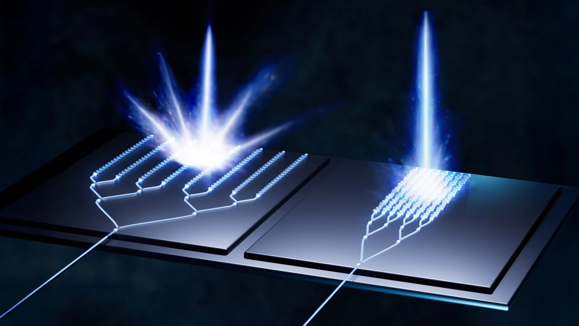
At the very core of this groundbreaking technology lie high-frequency microwave vibrations, oscillating at an astonishing rate of billions of times per second. These rapid oscillations are the secret sauce that empowers the chip to manipulate laser light with an unparalleled degree of precision. This fine-grained control over light is not merely an incremental improvement; it represents a fundamental shift in our ability to interact with and harness quantum phenomena.
By directly influencing the phase of a laser beam, the device can artfully generate new laser frequencies that are both exceptionally stable and highly efficient. This sophisticated level of control is not only a prerequisite for the successful operation of advanced quantum computers but also a vital enabler for burgeoning fields such as quantum sensing, which promises unprecedented accuracy in measurements, and quantum networking, which aims to create secure and powerful communication channels. The implications of this precise light manipulation extend far beyond the confines of quantum computing, touching upon a broad spectrum of scientific and technological frontiers.
Why Quantum Computers Need Ultra-Precise Lasers: The Delicate Dance of Qubits
To truly grasp the significance of this breakthrough, it’s imperative to understand the intricate workings of some of the most promising quantum computing architectures. Many of these designs hinge on the meticulous manipulation of trapped ions or trapped neutral atoms, each of which serves as an individual qubit, the fundamental building block of quantum information. The process of encoding and processing information in these systems involves directing precisely tuned laser beams at these atomic qubits. These laser interactions are akin to giving instructions, guiding the atoms through complex calculations. The sheer sensitivity of these quantum states necessitates an extraordinary level of precision in the laser control, often requiring adjustments within billionths of a percent.
"Creating new copies of a laser with very exact differences in frequency is one of the most important tools for working with atom- and ion-based quantum computers," Freedman eloquently explained. "But to do that at scale, you need technology that can efficiently generate those new frequencies." This statement underscores the core challenge that the researchers have so effectively addressed: the transition from laboratory curiosities to practical, scalable quantum systems.
Historically, achieving these precise frequency shifts has relied on large, cumbersome, table-top devices that consume substantial amounts of microwave power. While these existing systems have proven invaluable for proof-of-concept experiments and small-scale demonstrations, their sheer size, power demands, and complexity render them entirely impractical for the vast number of optical channels that will be required to orchestrate the millions of qubits envisioned for future quantum computers. The idea of filling an entire warehouse with these bulky optical tables to power a large-scale quantum machine is simply not feasible.
Professor Eichenfield vividly illustrated this point: "You’re not going to build a quantum computer with 100,000 bulk electro-optic modulators sitting in a warehouse full of optical tables. You need some much more scalable ways to manufacture them that don’t have to be hand-assembled and with long optical paths. While you’re at it, if you can make them all fit on a few small microchips and produce 100 times less heat, you’re much more likely to make it work." This statement encapsulates the engineering imperative driving the research: miniaturization, scalability, efficiency, and integration.
Lower Power Use, Less Heat, More Qubits: A Paradigm Shift in Efficiency
The newly developed device represents a monumental leap forward in terms of efficiency. It generates laser frequency shifts through highly efficient phase modulation, all while consuming approximately 80 times less microwave power compared to many existing commercial modulators. This dramatic reduction in power consumption has a cascade of beneficial effects. Most importantly, lower power usage translates directly into less heat generation. This reduction in thermal load is critical, as it allows for a much higher density of optical channels to be packed closely together, potentially even onto a single, compact microchip.
When viewed collectively, these advantages transform the humble chip into a sophisticated and scalable system. It is now capable of orchestrating the ultra-precise interactions that atoms require to perform complex quantum calculations, a feat that was previously hindered by the limitations of existing technologies. This enhanced efficiency not only reduces operational costs but also opens up new possibilities for the physical design and deployment of quantum computing hardware.
Built With the Same Technology as Modern Microchips: Harnessing the Power of CMOS Fabrication
Perhaps one of the most significant triumphs of this project is the fact that the device was entirely manufactured within a fabrication facility, or "fab." This is the same cutting-edge environment that is responsible for producing the advanced microelectronics that power our modern world, from the processors in our smartphones to the integrated circuits in our vehicles. This choice of manufacturing methodology is a game-changer.
"CMOS fabrication is the most scalable technology humans have ever invented," Professor Eichenfield stated with conviction. CMOS (Complementary Metal-Oxide-Semiconductor) is the ubiquitous semiconductor manufacturing process that underpins virtually all modern microelectronics.
He elaborated further, "Every microelectronic chip in every cell phone or computer has billions of essentially identical transistors on it. So, by using CMOS fabrication, in the future, we can produce thousands or even millions of identical versions of our photonic devices, which is exactly what quantum computing will need." This analogy highlights the immense potential for mass production and the uniformity that can be achieved, ensuring that each manufactured device performs to the same high standards.
According to Otterstrom, the team undertook the ambitious task of taking modulator technologies that were once characterized as bulky, prohibitively expensive, and power-intensive, and ingeniously redesigned them. The result is a device that is not only significantly smaller but also remarkably more efficient and substantially easier to integrate into larger systems.
Otterstorm aptly summarized this transformative effort: "We’re helping to push optics into its own ‘transistor revolution,’ moving away from the optical equivalent of vacuum tubes and towards scalable integrated photonic technologies." This powerful analogy draws a parallel to the groundbreaking invention of the transistor, which revolutionized electronics by replacing bulky and inefficient vacuum tubes with compact and reliable solid-state devices.
Toward Fully Integrated Quantum Photonic Chips: The Final Frontier
The research team is not resting on their laurels; they are actively pushing the boundaries of what’s possible. Their current focus is on developing fully integrated photonic circuits. These advanced circuits will elegantly combine multiple essential functions, including frequency generation, filtering, and pulse shaping, all onto a single, compact chip. This ambitious undertaking represents a crucial step towards realizing a complete, self-contained, and operational quantum photonic platform.
Looking ahead, the team has ambitious plans to forge strategic partnerships with leading quantum computing companies. These collaborations will be instrumental in testing and validating these newly developed chips within state-of-the-art trapped-ion and trapped-neutral-atom quantum computers. This real-world testing will provide invaluable feedback and accelerate the integration of this technology into practical quantum systems.
"This device is one of the final pieces of the puzzle," Freedman expressed with palpable excitement. "We’re getting close to a truly scalable photonic platform capable of controlling very large numbers of qubits." This sentiment underscores the feeling of nearing a significant breakthrough and the culmination of years of dedicated research and development.
The pioneering work described in this article was made possible through the generous support of the U.S. Department of Energy, specifically through the Quantum Systems Accelerator program, a distinguished National Quantum Initiative Science Research Center. This funding has been instrumental in fostering an environment of innovation and collaboration, driving forward the frontiers of quantum science and technology.