A groundbreaking collaboration between engineers from Stanford University, Carnegie Mellon University, the University of Pennsylvania, and the Massachusetts Institute of Technology, in partnership with SkyWater Technology, the nation’s largest exclusively U.S.-based pure-play semiconductor foundry, has culminated in the creation of a novel multilayer computer chip. This pioneering architecture promises to usher in a new era for AI hardware and significantly bolster American leadership in semiconductor innovation.
The fundamental departure from conventional, largely two-dimensional chips lies in the new prototype’s vertical construction. Imagine a towering skyscraper where ultra-thin components are stacked like floors, and a sophisticated network of vertical wiring acts as high-speed elevators, facilitating the rapid transit of vast quantities of data. This innovative design boasts a record-breaking number of vertical connections and an exceptionally dense, interwoven layout that strategically places memory and computing units in close proximity. This proximity is crucial, as it effectively bypasses the debilitating slowdowns that have plagued the progress of flat, 2D chips. In rigorous hardware tests and sophisticated simulations, this advanced 3D chip has demonstrated performance improvements that are roughly an order of magnitude greater than its 2D counterparts.
While the concept of experimental 3D chips has been explored in academic settings for some time, this latest development marks a significant milestone: it is the first time such a chip has delivered demonstrable performance enhancements and, critically, has been produced within a commercial foundry environment. "This opens the door to a new era of chip production and innovation," declared Subhasish Mitra, the William E. Ayer Professor in Electrical Engineering and professor of computer science at Stanford University, and the principal investigator of the research paper detailing this achievement, which was presented at the 71st Annual IEEE International Electron Devices Meeting (IEDM). "Breakthroughs like this are how we get to the 1,000-fold hardware performance improvements future AI systems will demand."
The Achilles’ Heel of Flat Chips in the Age of Modern AI
The insatiable appetite of large artificial intelligence models, such as ChatGPT and Claude, for data presents a formidable challenge. These sophisticated systems are in a perpetual state of shuttling enormous volumes of information between memory, where data is stored, and the computing units, responsible for its processing.
On traditional 2D chips, where all components reside on a single surface, memory is inherently limited and often dispersed. This spatial limitation forces data to traverse a constricted network of long, congested pathways. Consequently, the processing units, capable of operating at lightning-fast speeds, frequently find themselves waiting for data, as the chip’s infrastructure cannot deliver it quickly enough. Furthermore, the chip struggles to maintain sufficient memory in close proximity to these compute-intensive operations. This perpetual state of waiting is colloquially known as the "memory wall," a critical bottleneck where processing speed outstrips the chip’s ability to supply the necessary data.
For years, the semiconductor industry has strived to push back against this memory wall by relentlessly shrinking transistors – the minuscule switches that perform computations and store data – and by cramming ever-greater numbers of them onto each chip. However, researchers now assert that this approach is approaching its fundamental physical limitations, often referred to as the "miniaturization wall."
The newly developed 3D chip design offers a compelling solution to surmount both these formidable obstacles by embracing verticality. "By integrating memory and computation vertically, we can move a lot more information much quicker, just as the elevator banks in a high-rise let many residents travel between floors at once," explained Tathagata Srimani, assistant professor of electrical and computer engineering at Carnegie Mellon University and the paper’s senior author, who initiated this work as a postdoctoral fellow under Mitra’s guidance.
Robert M. Radway, assistant professor of electrical and systems engineering at the University of Pennsylvania and a co-author of the study, elaborated on the critical challenge: "The memory wall and the miniaturization wall form a deadly combination. We attacked it head-on by tightly integrating memory and logic and then building upward at extremely high density. It’s like the Manhattan of computing — we can fit more people in less space."
The Manufacturing Marvel: Crafting the Monolithic 3D Chip
Many prior attempts at creating 3D chips have adopted a more rudimentary approach, involving the stacking of pre-fabricated, separate chips. While this method can offer some advantages, the inter-layer connections are often less refined, limited in number, and can themselves become significant bottlenecks.
This research team, however, pursued a distinctly different and more sophisticated methodology. Instead of manufacturing individual chips and subsequently bonding them together, they meticulously build each new layer directly atop the preceding one in a seamless, continuous manufacturing flow. This technique, termed "monolithic" 3D integration, employs temperatures sufficiently low to prevent any damage to the circuitry already established in the layers below. This critical capability enables the layers to be stacked with unprecedented closeness and facilitates the creation of a far denser network of interconnections between them.
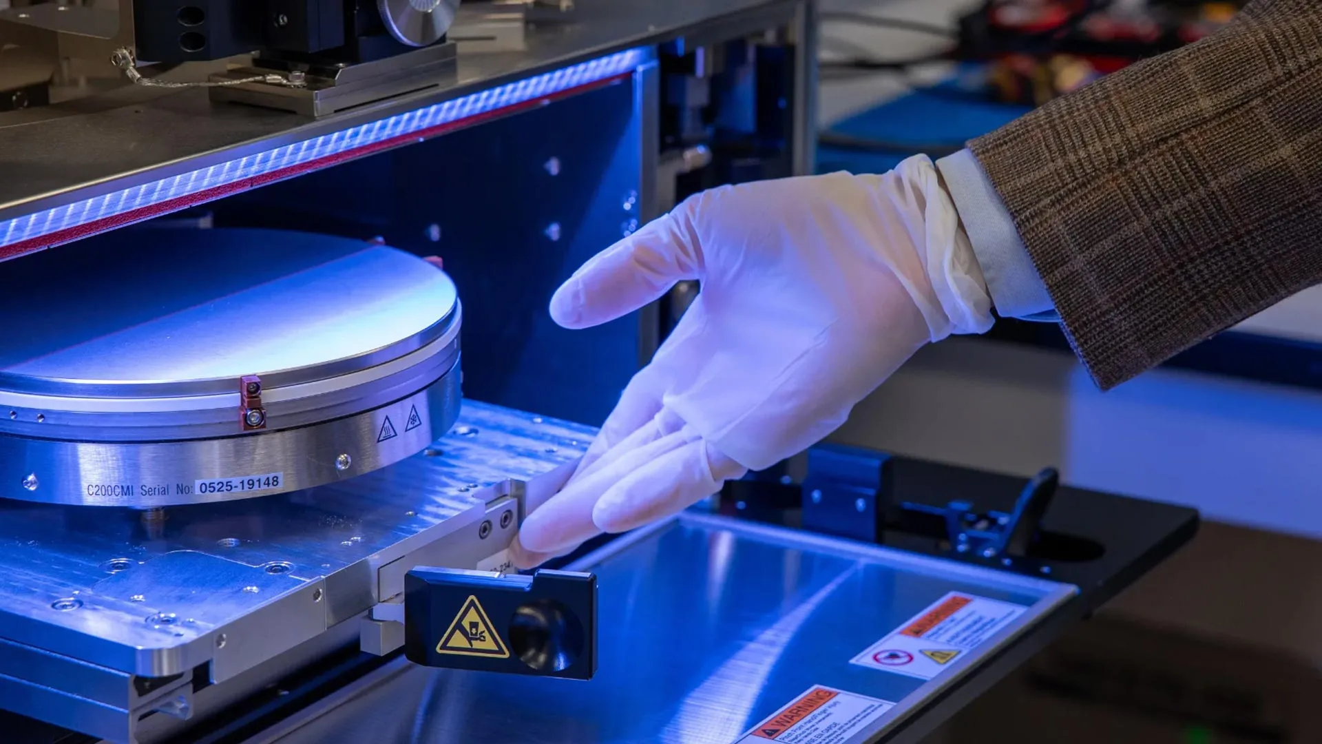
A pivotal aspect of this breakthrough, as emphasized by the researchers, is that the entire manufacturing process was successfully executed within a domestic commercial silicon foundry. "Turning a cutting-edge academic concept into something a commercial fab can build is an enormous challenge," stated co-author Mark Nelson, vice president of technology development operations at SkyWater Technology. "This shows that these advanced architectures aren’t just possible in the lab — they can be produced domestically, at scale, which is what America needs to stay at the forefront of semiconductor innovation."
Tangible Performance Gains and the Future Trajectory of AI Hardware
Initial hardware tests have yielded impressive results, with the prototype outperforming comparable 2D chips by approximately fourfold. Furthermore, the team’s extensive simulations suggest even more dramatic performance enhancements as the design is scaled up, incorporating additional stacked layers of memory and compute. Projections indicate that with further tiers, the models could achieve up to a twelve-fold improvement on real-world AI workloads, including those derived from Meta’s open-source LLaMA model.
Beyond these immediate performance gains, the researchers highlight a more profound, long-term benefit. They posit that this architecture offers a viable pathway to achieving a staggering 100 to 1,000-fold improvement in the Energy Delay Product (EDP). EDP is a critical metric that encapsulates both the speed of computation and its energy efficiency. By drastically reducing the distances data must travel and introducing a multitude of vertical pathways for its movement, the chip can simultaneously boost throughput and decrease the energy consumed per operation – a synergistic combination that has proven exceptionally elusive with conventional flat designs.
The significance of this work extends beyond mere performance metrics. By demonstrating the feasibility of manufacturing monolithic 3D chips within the United States, the team is providing a compelling blueprint for a new era of domestic hardware innovation. This could enable the design and production of the most advanced chips on American soil, fostering a more resilient and competitive semiconductor ecosystem.
Moreover, the researchers anticipate that this paradigm shift towards vertical, monolithic 3D integration will necessitate the cultivation of a new generation of engineers proficient in these advanced methodologies. This mirrors the transformative impact of the integrated circuit boom in the 1980s, which was fueled by students acquiring expertise in chip design and fabrication within U.S. laboratories. Through strategic collaborations and dedicated funding initiatives, such as the Microelectronics Commons California-Pacific-Northwest AI Hardware Hub (Northwest-AI-Hub), students and researchers are already being actively prepared to propel American semiconductor innovation forward.
"Breakthroughs like this are of course about performance," affirmed H.-S. Philip Wong, the Willard R. and Inez Kerr Bell Professor in the Stanford School of Engineering and principal investigator of the Northwest-AI-Hub. "But they’re also about capability. If we can build advanced 3D chips, we can innovate faster, respond faster, and shape the future of AI hardware."
This seminal research was conducted across the Stanford University School of Engineering, Carnegie Mellon University College of Engineering, the University of Pennsylvania School of Engineering and Applied Science, and the Massachusetts Institute of Technology. All fabrication was meticulously carried out at SkyWater Technology’s Bloomington, Minnesota, Foundry. The project received crucial support from a consortium of esteemed organizations, including the Defense Advanced Research Projects Agency, the U.S. National Science Foundation Graduate Research Fellowship Program, Samsung, the Stanford Precourt Institute for Energy, the Stanford SystemX Alliance, the Department of War’s Microelectronics Commons AI Hardware Hub, the U.S. Department of Energy, and the National Science Foundation’s Future of Semiconductors Program (grant number 2425218).
Additional contributing Stanford co-authors include Suhyeong Choi, Samuel Dayo, Andrew Bechdolt, Shengman Li, Dennis T. Rich, and R.H. Yang. Further collaborators on this project hail from Carnegie Mellon University and the Massachusetts Institute of Technology, underscoring the truly inter-institutional nature of this significant advancement.