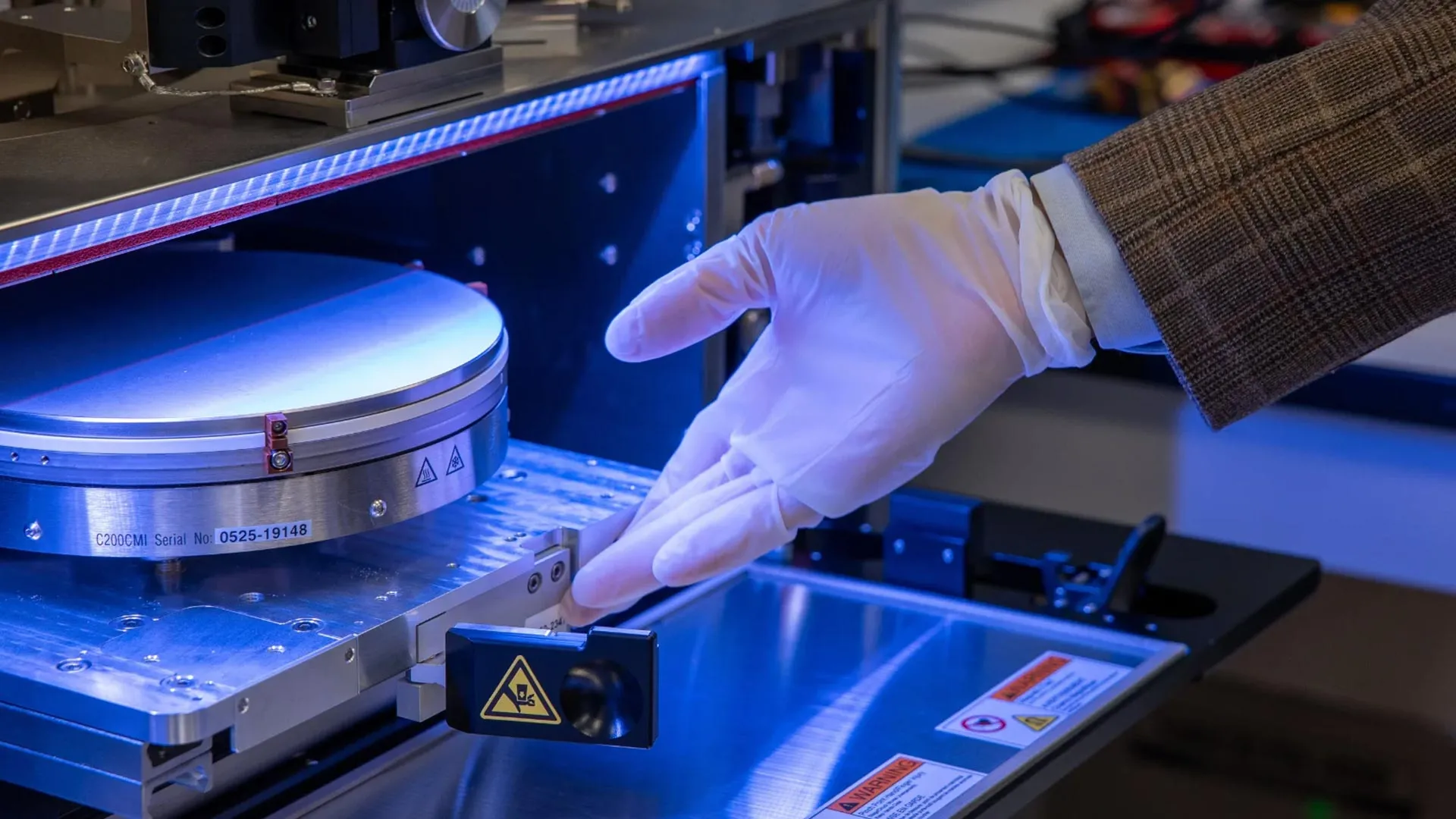
In a groundbreaking development poised to revolutionize artificial intelligence hardware and bolster domestic semiconductor capabilities, a collaborative team of engineers from Stanford University, Carnegie Mellon University, the University of Pennsylvania, and the Massachusetts Institute of Technology has unveiled a novel multilayered computer chip. Working in conjunction with SkyWater Technology, the nation’s largest dedicated U.S.-based pure-play semiconductor foundry, this innovation represents a significant departure from the predominantly flat, two-dimensional architecture of current chips, offering a vertically integrated design that promises to overcome critical performance limitations in AI processing.
The newly developed prototype is engineered with a unique, upward-growing structure, akin to the layered floors of a skyscraper. This intricate design employs ultra-thin components stacked vertically, interconnected by an extensive network of high-speed vertical wiring that functions as a hyper-efficient data transportation system, capable of moving vast quantities of information with unprecedented speed. The chip boasts a record-breaking number of vertical connections and a meticulously interwoven layout that strategically positions memory and computing units in close proximity. This proximity is crucial, as it effectively eliminates the performance slowdowns that have long plagued conventional flat chips, a phenomenon often referred to as the "memory wall." In rigorous hardware tests and sophisticated simulations, this 3D chip has demonstrated performance gains that are roughly an order of magnitude superior to its 2D counterparts.
While experimental 3D chips have been explored in academic settings previously, this project marks the first instance where a 3D chip has not only delivered tangible performance improvements but has also been manufactured within a commercial foundry. Subhasish Mitra, the William E. Ayer Professor in Electrical Engineering and Professor of Computer Science at Stanford University, and the principal investigator of the research paper detailing this breakthrough, presented at the 71st Annual IEEE International Electron Devices Meeting (IEDM), stated, "This opens the door to a new era of chip production and innovation. Breakthroughs like this are how we get to the 1,000-fold hardware performance improvements future AI systems will demand."
The inherent limitations of flat chips in handling the demands of modern AI are well-documented. Large-scale AI models, such as those powering ChatGPT and Claude, necessitate the constant and rapid shuttling of enormous datasets between memory modules, which store information, and the processing units responsible for computation. In conventional 2D chip architectures, where all components reside on a single plane, memory is inherently limited and often dispersed. This necessitates data to traverse long, congested pathways, creating a bottleneck. The computing units, capable of processing data at exceptionally high speeds, often find themselves waiting for data to arrive, as the chip’s ability to deliver information and maintain sufficient nearby memory is constrained. This persistent waiting game is the essence of the "memory wall."
For years, the semiconductor industry has attempted to circumvent the memory wall by progressively shrinking transistors – the fundamental building blocks of chips that perform computations and store data – thereby increasing their density on each chip. However, researchers now acknowledge that this approach is rapidly approaching its physical limits, a challenge known as the "miniaturization wall." The newly developed 3D chip design directly addresses both of these formidable barriers by embracing vertical integration.
Tathagata Srimani, Assistant Professor of Electrical and Computer Engineering at Carnegie Mellon University and the paper’s senior author, who initiated this research as a postdoctoral fellow under Mitra’s guidance, explained the analogy: "By integrating memory and computation vertically, we can move a lot more information much quicker, just as the elevator banks in a high-rise let many residents travel between floors at once."
Robert M. Radway, Assistant Professor of Electrical and Systems Engineering at the University of Pennsylvania and a co-author of the study, elaborated on the synergistic challenge: "The memory wall and the miniaturization wall form a deadly combination. We attacked it head-on by tightly integrating memory and logic and then building upward at extremely high density. It’s like the Manhattan of computing — we can fit more people in less space."
The manufacturing process for this monolithic 3D chip represents a significant advancement over previous 3D integration efforts. Many earlier attempts involved stacking separate, pre-fabricated chips. While this offered some benefits, the interconnections between these stacked layers were often rudimentary, limited in number, and prone to becoming bottlenecks. The current team, however, employed a more sophisticated "monolithic" 3D integration technique. Instead of bonding separate chips, each new layer is meticulously fabricated directly on top of the preceding one in a continuous, seamless process. This method is enabled by maintaining temperatures low enough to prevent damage to the already constructed circuitry below. This allows for significantly denser layering and a far greater number of interconnections between these layers.
A particularly crucial aspect of this achievement, according to the researchers, is that the entire manufacturing process was conducted within a domestic commercial silicon foundry. Mark Nelson, Vice President of Technology Development Operations at SkyWater Technology and a co-author, emphasized the significance: "Turning a cutting-edge academic concept into something a commercial fab can build is an enormous challenge. This shows that these advanced architectures aren’t just possible in the lab — they can be produced domestically, at scale, which is what America needs to stay at the forefront of semiconductor innovation."
The performance gains observed in early hardware tests have been substantial, with the prototype outperforming comparable 2D chips by approximately fourfold. Furthermore, the team’s simulations project even more dramatic improvements as the design is scaled up with additional stacked layers of memory and compute. These simulations suggest that with further tiers, the design could achieve up to a twelvefold improvement on real-world AI workloads, including those derived from Meta’s open-source LLaMA model.
Beyond immediate performance enhancements, the researchers highlight a more profound, long-term payoff. The proposed architecture offers a viable pathway to achieving an energy-delay product (EDP) improvement of 100 to 1,000 times. EDP is a critical metric that encapsulates both the speed of computation and its energy efficiency. By drastically reducing the distances data must travel and providing a multitude of high-speed vertical pathways, the chip can simultaneously boost throughput and decrease the energy consumed per operation – a feat that has proven exceedingly difficult with conventional flat designs.
The importance of this work extends beyond mere technical performance. By successfully demonstrating that monolithic 3D chips can be manufactured in the United States, the team provides a compelling blueprint for a new era of domestic hardware innovation. This paves the way for the design and production of the most advanced chips on American soil, fostering technological sovereignty.
Moreover, the transition to vertical, monolithic 3D integration will necessitate a new generation of engineers proficient in these advanced manufacturing techniques. This mirrors the impact of the integrated circuit revolution in the 1980s, which was propelled by students acquiring chip design and fabrication expertise in U.S. laboratories. Through collaborative initiatives and dedicated funding efforts, such as those supporting the Microelectronics Commons California-Pacific-Northwest AI Hardware Hub (Northwest-AI-Hub), students and researchers are already being actively trained to drive American semiconductor innovation forward.
H.-S. Philip Wong, the Willard R. and Inez Kerr Bell Professor in the Stanford School of Engineering and principal investigator of the Northwest-AI-Hub, articulated the broader implications: "Breakthroughs like this are of course about performance. But they’re also about capability. If we can build advanced 3D chips, we can innovate faster, respond faster, and shape the future of AI hardware."
This pioneering research was conducted across the Stanford University School of Engineering, Carnegie Mellon University College of Engineering, the University of Pennsylvania School of Engineering and Applied Science, and the Massachusetts Institute of Technology. All fabrication was completed at SkyWater Technology’s foundry in Bloomington, Minnesota. The project received crucial support from a diverse range of organizations, including the Defense Advanced Research Projects Agency, the U.S. National Science Foundation Graduate Research Fellowship Program, Samsung, the Stanford Precourt Institute for Energy, the Stanford SystemX Alliance, the Department of War’s Microelectronics Commons AI Hardware Hub, the U.S. Department of Energy, and the National Science Foundation’s Future of Semiconductors Program (grant number 2425218). Additional Stanford co-authors on the study include Suhyeong Choi, Samuel Dayo, Andrew Bechdolt, Shengman Li, Dennis T. Rich, and R.H. Yang, with further contributions from researchers at Carnegie Mellon University and MIT.